Semiconductor device and method for manufacturing the same

a semiconductor integrated circuit and semiconductor technology, applied in the direction of semiconductor devices, electrical equipment, transistors, etc., can solve problems such as leakage, and achieve the effect of reducing leakag

Active Publication Date: 2013-06-06
SEMICON ENERGY LAB CO LTD
View PDF6 Cites 61 Cited by
  • Summary
  • Abstract
  • Description
  • Claims
  • Application Information

AI Technical Summary

Benefits of technology

[0014]A shorter channel length causes the problem of leakage due to a parasitic channel. Therefore, it is an object to provide a transistor structure for reducing the leakage due to a parasitic

Problems solved by technology

A shorter channel length causes the probl

Method used


Image

  • Semiconductor device and method for manufacturing the same
  • Semiconductor device and method for manufacturing the same
  • Semiconductor device and method for manufacturing the same

Examples


embodiment 1

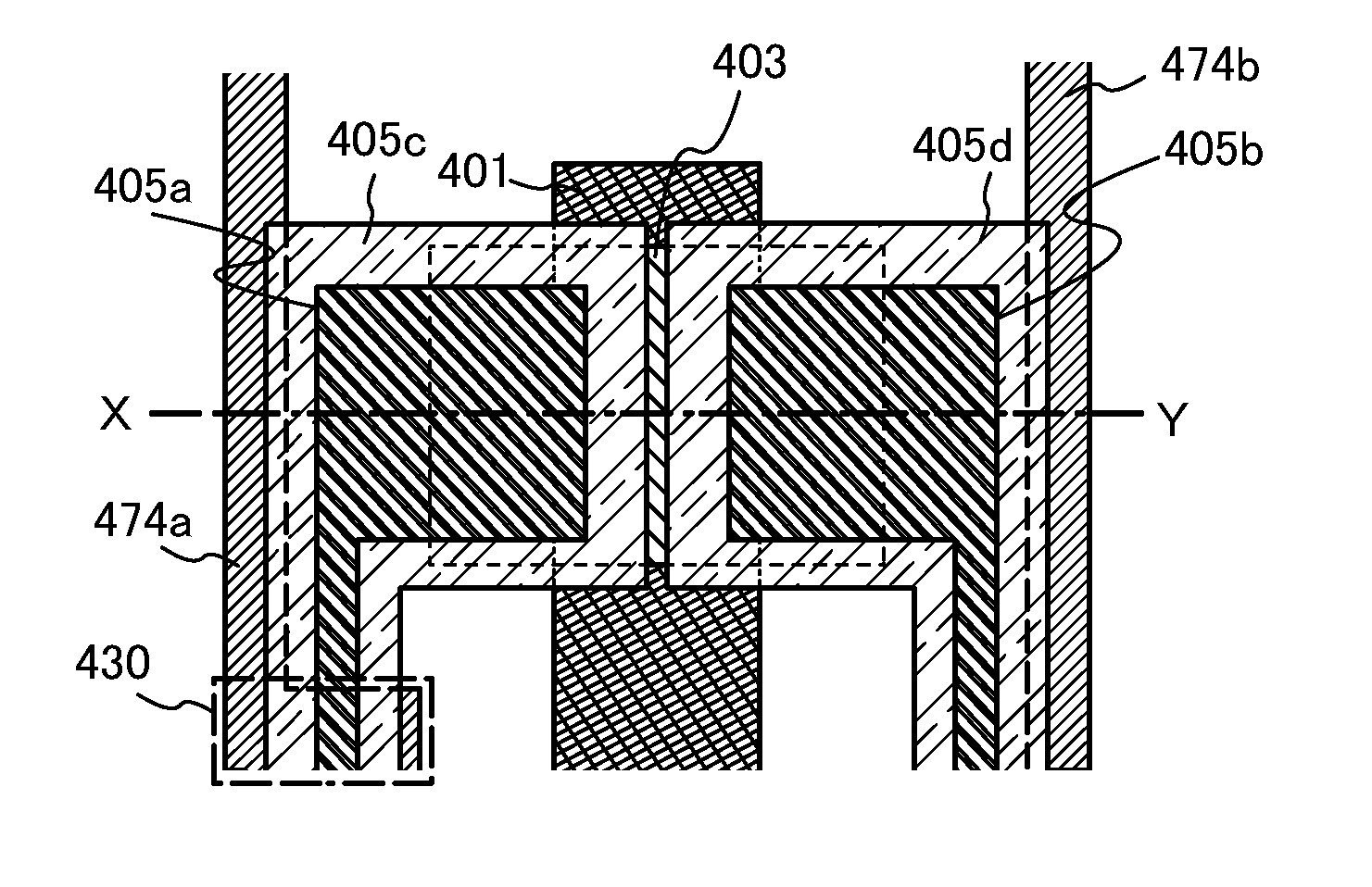
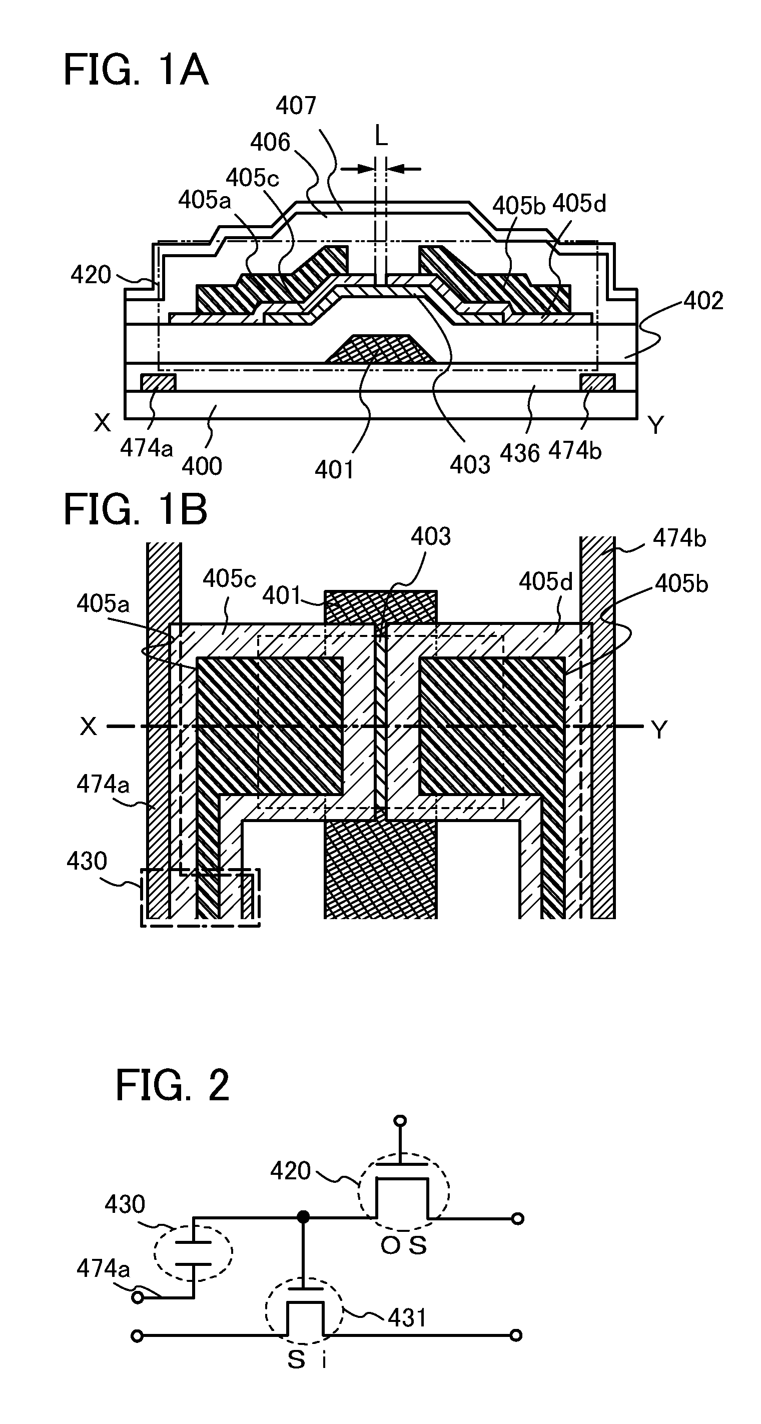
[0066]In this embodiment, one embodiment of a semiconductor device will be described with reference to FIGS. 1A and 1B. FIG. 1B is a top view of a transistor 420, and FIG. 1A is a cross-sectional view taken along X-Y in FIG. 1B.

[0067]The transistor 420 illustrated in FIGS. 1A and 1B includes a base insulating layer 436 over a substrate 400, a gate electrode layer 401 over the base insulating layer 436, a gate insulating layer 402 over the gate electrode layer 401, an oxide semiconductor layer 403 over the gate electrode layer 401 with the gate insulating layer 402 provided therebetween, a drain electrode layer and a source electrode layer, and an insulating layer 406 and an insulating layer 407 over the oxide semiconductor layer 403. Note that portions in the oxide semiconductor layer 403, which the drain electrode layer and the source electrode layer are in contact with, and their vicinity may have lower resistivity than in other portions in the oxide semiconductor layer 403, and t...

embodiment 2

[0120]In this embodiment, a semiconductor device of another embodiment, which is different from the semiconductor device described in Embodiment 1, and a method for manufacturing the semiconductor device will be described.

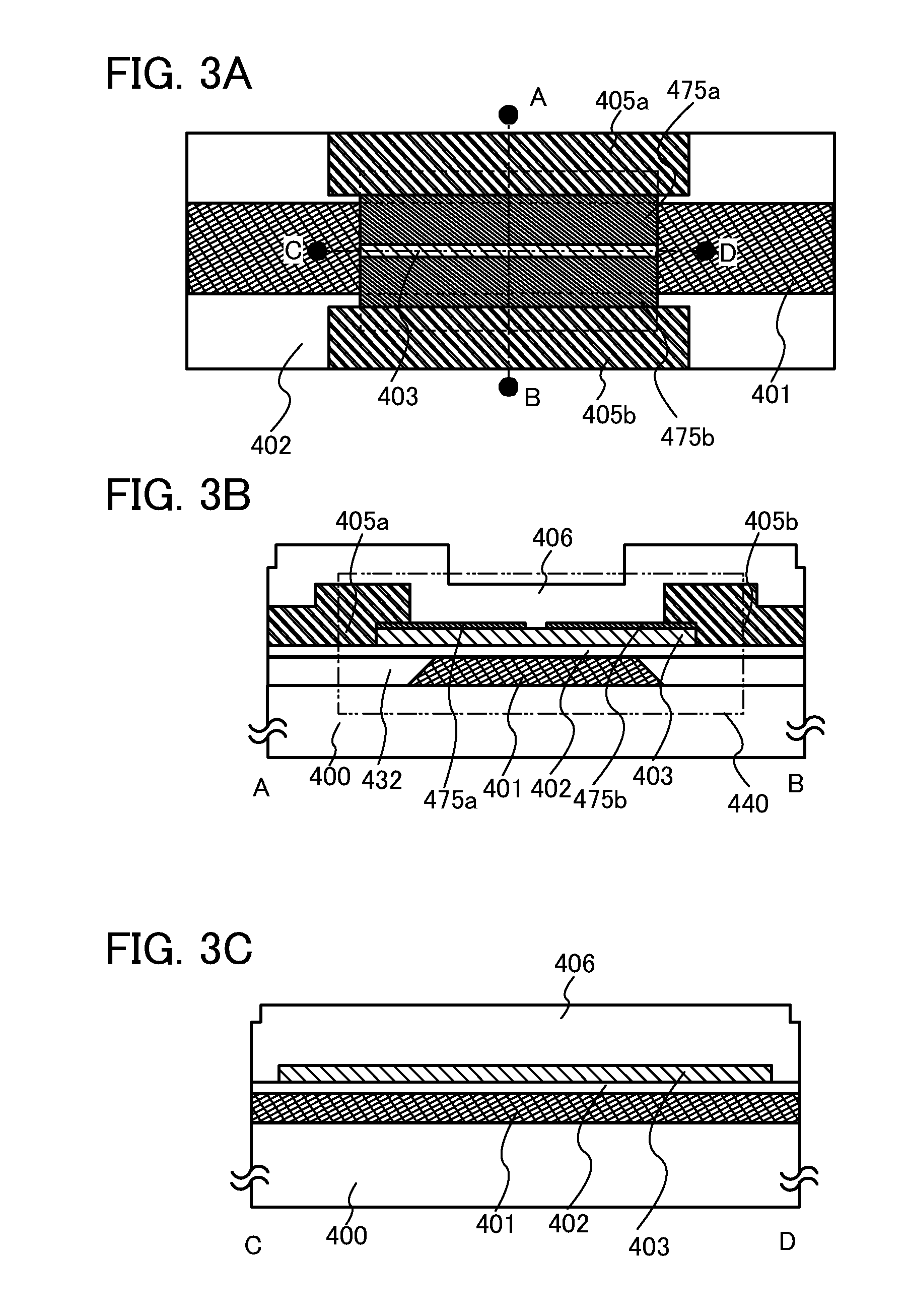
[0121]FIGS. 3A to 3C illustrate the semiconductor device of this embodiment. FIG. 3A is a top view of a transistor included in the semiconductor device of this embodiment. FIG. 3B is a cross-sectional view taken along A-B (channel length direction) in FIG. 3A. FIG. 3C is a cross-sectional view taken along C-D in FIG. 3A. Note that some components illustrated in FIG. 3B or 3C are not illustrated in FIG. 3A for simplicity of the drawing.

[0122]Note that, in this embodiment, portions that are similar to the portions in Embodiment 1 are denoted by the same reference numerals in the drawings, and detailed description thereof is omitted.

[0123]A transistor 440 illustrated in FIGS. 3A to 3C includes a gate electrode layer 401 over a substrate 400, an insulating layer 432 wh...

embodiment 3

[0206]In this embodiment, a structure of a semiconductor device in one embodiment of the present invention, which is different from those in Embodiments 1 and 2, will be described.

[0207]FIGS. 13A to 13C illustrate the semiconductor device of this embodiment. FIG. 13A is a top view of a transistor included in the semiconductor device of this embodiment. FIG. 13B is a cross-sectional view taken along E-F (channel length direction) in FIG. 13A. FIG. 13C is a cross-sectional view taken along G-H in FIG. 13A. Note that some components illustrated in FIG. 13B or 13C are not illustrated in FIG. 13A for simplicity of the drawing.

[0208]Note that, in this embodiment, portions that are similar to the portions in Embodiments 1 and 2 are denoted by the same reference numerals in the drawings, and detailed description thereof is omitted.

[0209]A transistor 460 illustrated in FIGS. 13A to 13C includes a gate electrode layer 401 over a substrate 400, an insulating layer 432 which is in contact with ...


PUM


Abstract

A semiconductor device including a minute transistor with a short channel length is provided. A gate insulating layer is formed over a gate electrode layer; an oxide semiconductor layer is formed over the gate insulating layer; a first conductive layer and a second conductive layer are formed over the oxide semiconductor layer; a conductive film is formed over the first conductive layer and the second conductive layer; a resist mask is formed over the conductive film by performing electron beam exposure; and then a third conductive layer and a fourth conductive layer are formed over and in contact with the first conductive layer and the second conductive layer, respectively, by selectively etching the conductive film.

Description

TECHNICAL FIELD[0001]The present invention relates to a technique for miniaturizing semiconductor integrated circuits. The invention disclosed in this specification includes in its scope an element formed using a compound semiconductor, in addition to that formed using a silicon semiconductor, as a component of a semiconductor integrated circuit, and discloses an element formed using a wide-gap semiconductor as an example.[0002]In this specification, a semiconductor device generally means a device which can function by utilizing semiconductor characteristics, and an electro-optic device, a semiconductor circuit, and an electronic device are all semiconductor devices.BACKGROUND ART[0003]As semiconductor memory devices, dynamic RAMs (DRAMs) formed using a silicon substrate are well-known products and currently used in a variety of electronic devices. A memory cell which is a key component in a DRAM includes a reading and writing transistor and a capacitor.[0004]DRAMs are an example of...

Claims


Application Information

Patent Timeline
IPC IPC(8): H01L29/786H01L29/66
CPCH01L29/786H01L29/7869H01L29/66969H01L29/66742H01L29/41733H01L29/78618
Inventor YAMAZAKI, SHUNPEIISOBE, ATSUOIEDA, YOSHINORINAGAI, MASAHARU
Owner SEMICON ENERGY LAB CO LTD
Why Eureka
Try Eureka