Superjunction Structures for Power Devices and Methods of Manufacture

Active Publication Date: 2009-03-26
SEMICON COMPONENTS IND LLC
View PDF110 Cites 203 Cited by
  • Summary
  • Abstract
  • Description
  • Claims
  • Application Information

AI Technical Summary

Benefits of technology

[0167]In one variation the post bake process results in silicon migration

Problems solved by technology

For example, in the case of the power MOSFET, because of the proportional relationship between the drain-to-source on-resistance R.su

Method used


Image

  • Superjunction Structures for Power Devices and Methods of Manufacture
  • Superjunction Structures for Power Devices and Methods of Manufacture
  • Superjunction Structures for Power Devices and Methods of Manufacture

Examples


Embodiment Construction

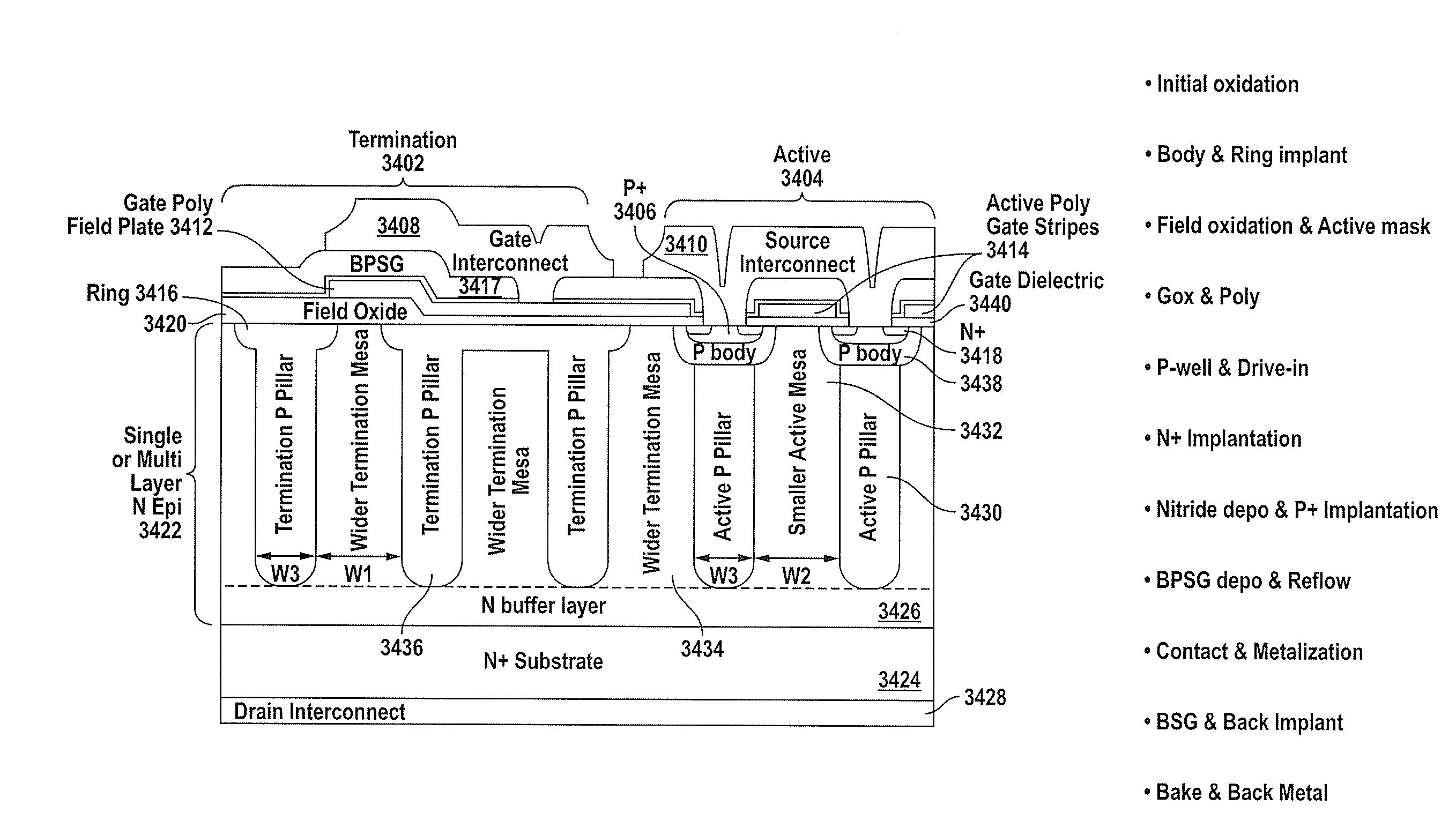
[0239]The power switch can be implemented by any one of power MOSFET, IGBT, various types of thyristors and the like. Many of the novel techniques presented herein are described in the context of the power MOSFET for illustrative purposes. It is to be understood however that the various embodiments of the invention described herein are not limited to the power MOSFET and can apply to many of the other types of power switch technologies, including, for example, IGBTs and other types of bipolar switches and various types of thyristors, as well as diodes. Further, for the purposes of illustration, the various embodiments of the invention are shown to include specific P and N type regions (e.g., for an n-channel MOSFET). It is understood by those skilled in the art that the teachings herein are equally applicable to devices in which the conductivities of the various regions are reversed

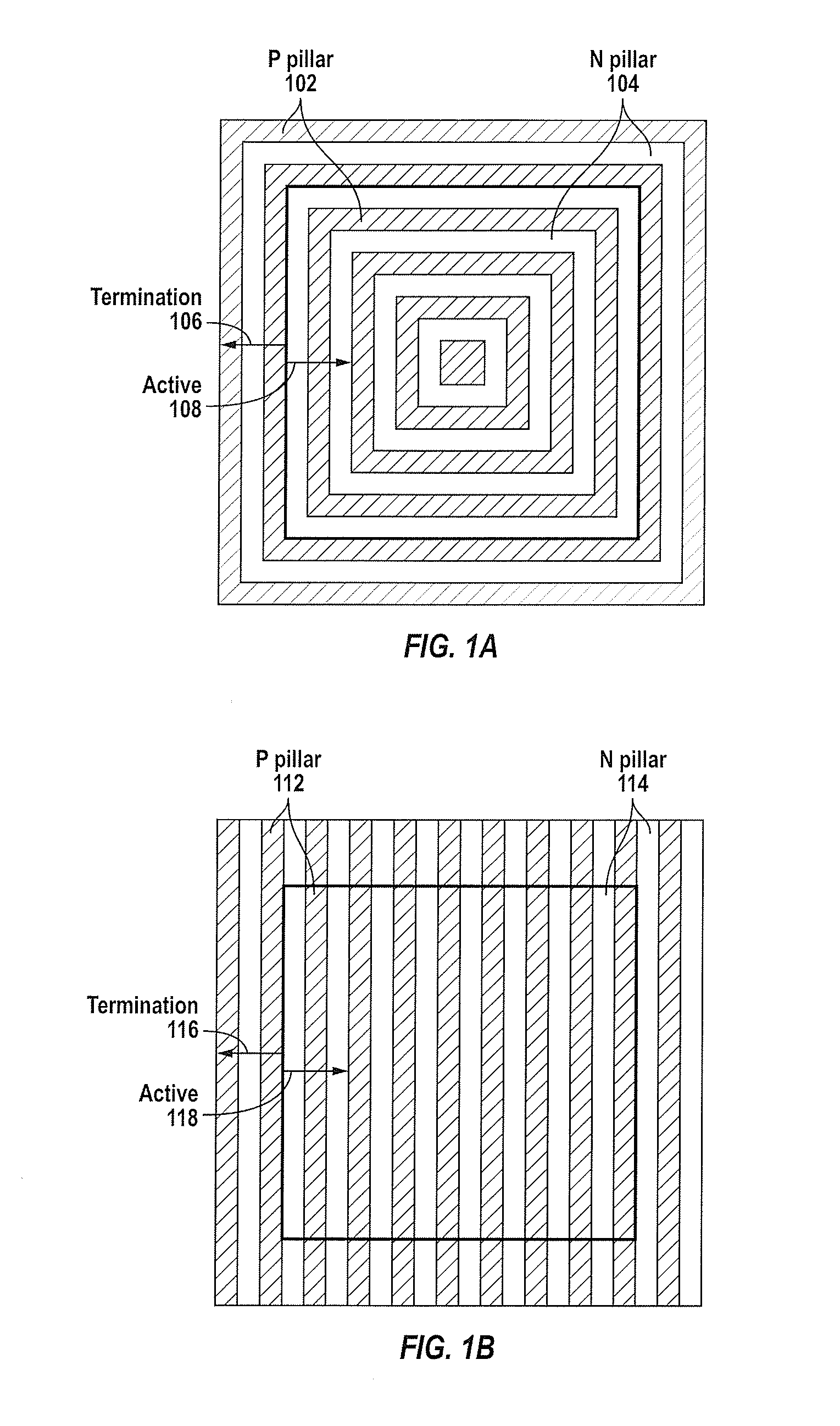
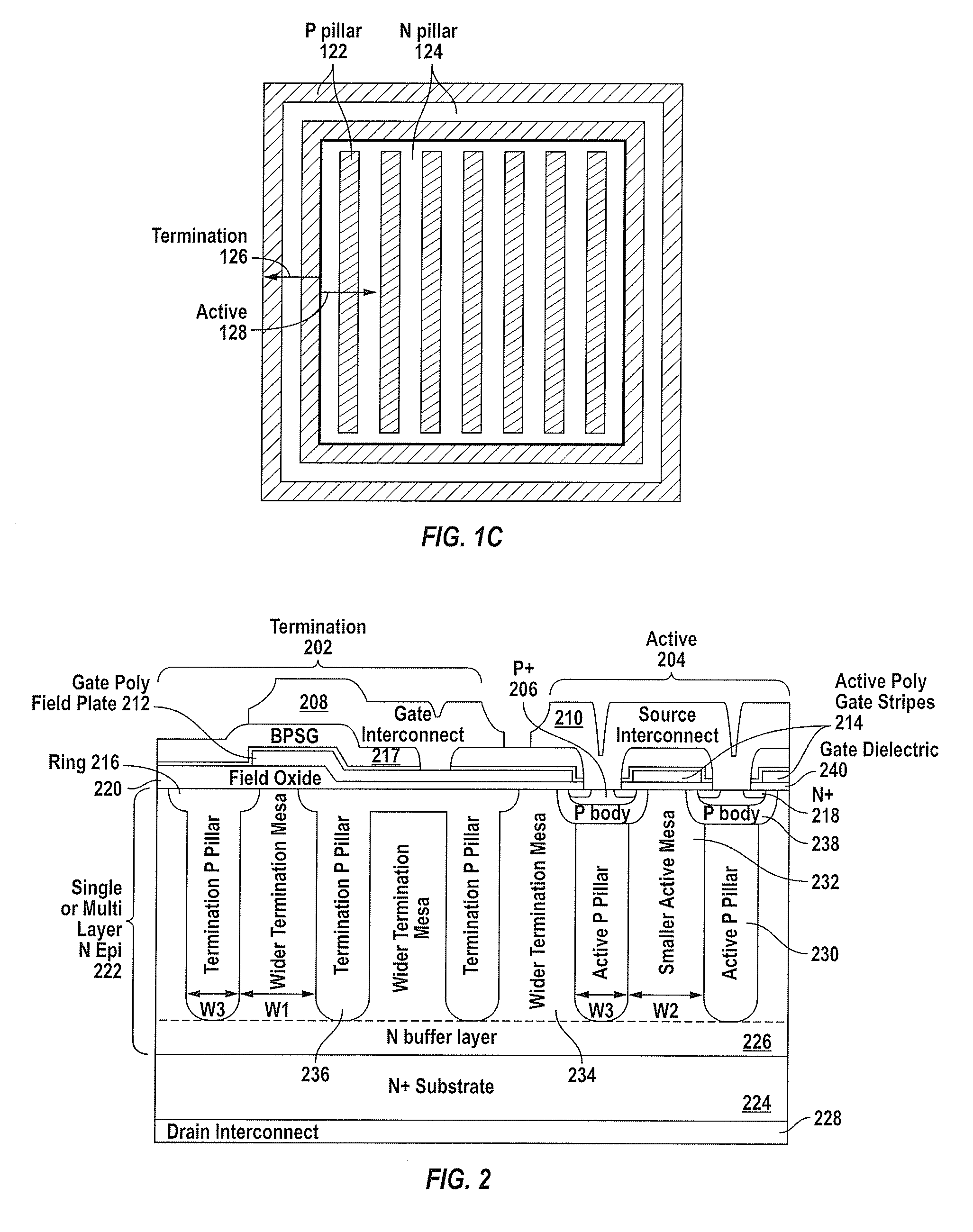
[0240]In the super-junction technology, the alternating P / N pillars 102 and 104 in the active and term...


PUM


Abstract

A power device includes an active region and a termination region surrounding the active region. A plurality of pillars of first and second conductivity type are alternately arranged in each of the active and termination regions. The pillars of first conductivity type in the active and termination regions have substantially the same width, and the pillars of second conductivity type in the active region have a smaller width than the pillars of second conductivity type in the termination region so that a charge balance condition in each of the active and termination regions results in a higher breakdown voltage in the termination region than in the active region.

Description

CROSS-REFERENCE TO RELATED APPLICATIONS[0001]This application claims the benefit of U.S. Provisional Appln. No. 60 / 974,433, filed Sep. 21, 2007, which is incorporated by reference in its entirety for all purposes.BACKGROUND OF THE INVENTION[0002]The present invention relates in general to semiconductor technology and in particular to various embodiments for improved power semiconductor devices such s transistors and diodes and their methods of manufacture.[0003]The key component in power electronic applications is the solid-state switch. From ignition control in automotive applications to battery-operated consumer electronic devices, to power converters in industrial applications, there is a need for a power switch that optimally meets the demands of the particular application. Solid-state switches including, for example, the power metal-oxide-semiconductor field effect transistor (power MOSFET), the insulated-gate bipolar transistor (IGBT) and various types of thyristors have conti...

Claims


Application Information

Patent Timeline
IPC IPC(8): H01L23/62
CPCH01L2924/0002H01L29/0634H01L29/66712H01L29/0696H01L29/1095H01L29/7813H01L29/0878H01L29/0615H01L29/404H01L29/7811H01L2924/00H01L21/02532H01L21/26513H01L21/30604H01L29/1075H01L29/7395H01L29/7397
Inventor LEE, JAEGILJANG, HOCHEOL
Owner SEMICON COMPONENTS IND LLC
Why Eureka
Try Eureka