Fully depleted soi device for reducing parasitic back gate capacitance

a back gate capacitance and fully depleted technology, applied in semiconductor devices, semiconductor/solid-state device details, electrical apparatus, etc., can solve problems such as poor breakdown performance, and achieve the effect of reducing parasitic back gate capacitan

Active Publication Date: 2018-04-05
IBM CORP
View PDF2 Cites 266 Cited by
  • Summary
  • Abstract
  • Description
  • Claims
  • Application Information

AI Technical Summary

Problems solved by technology

Shallow junctions are needed to avoid lateral diffusion of implanted dopants into the channel, since such diffusion disadvantageously contributes to leakage currents and poor breakdown performance.

Method used


Image

  • Fully depleted soi device for reducing parasitic back gate capacitance
  • Fully depleted soi device for reducing parasitic back gate capacitance
  • Fully depleted soi device for reducing parasitic back gate capacitance

Examples


Embodiment Construction

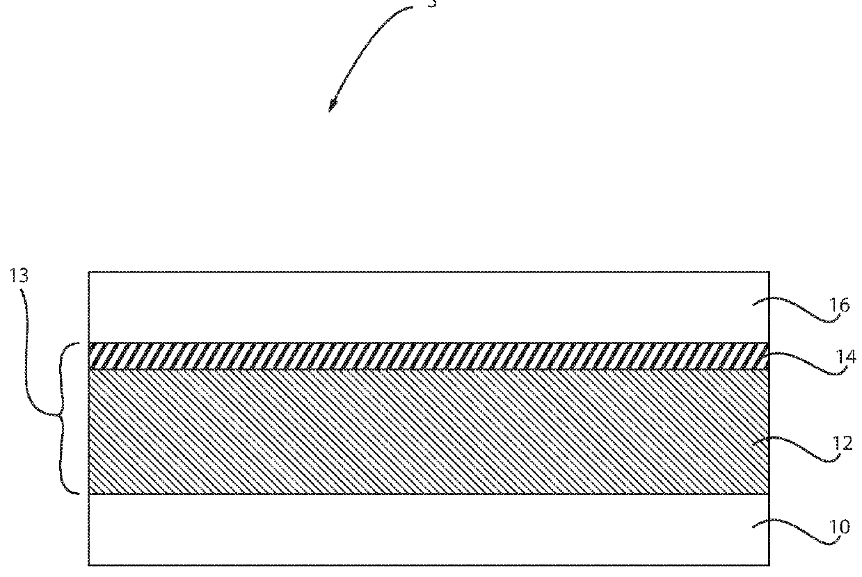
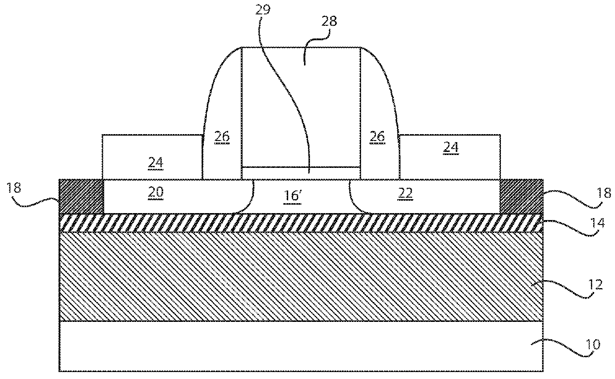
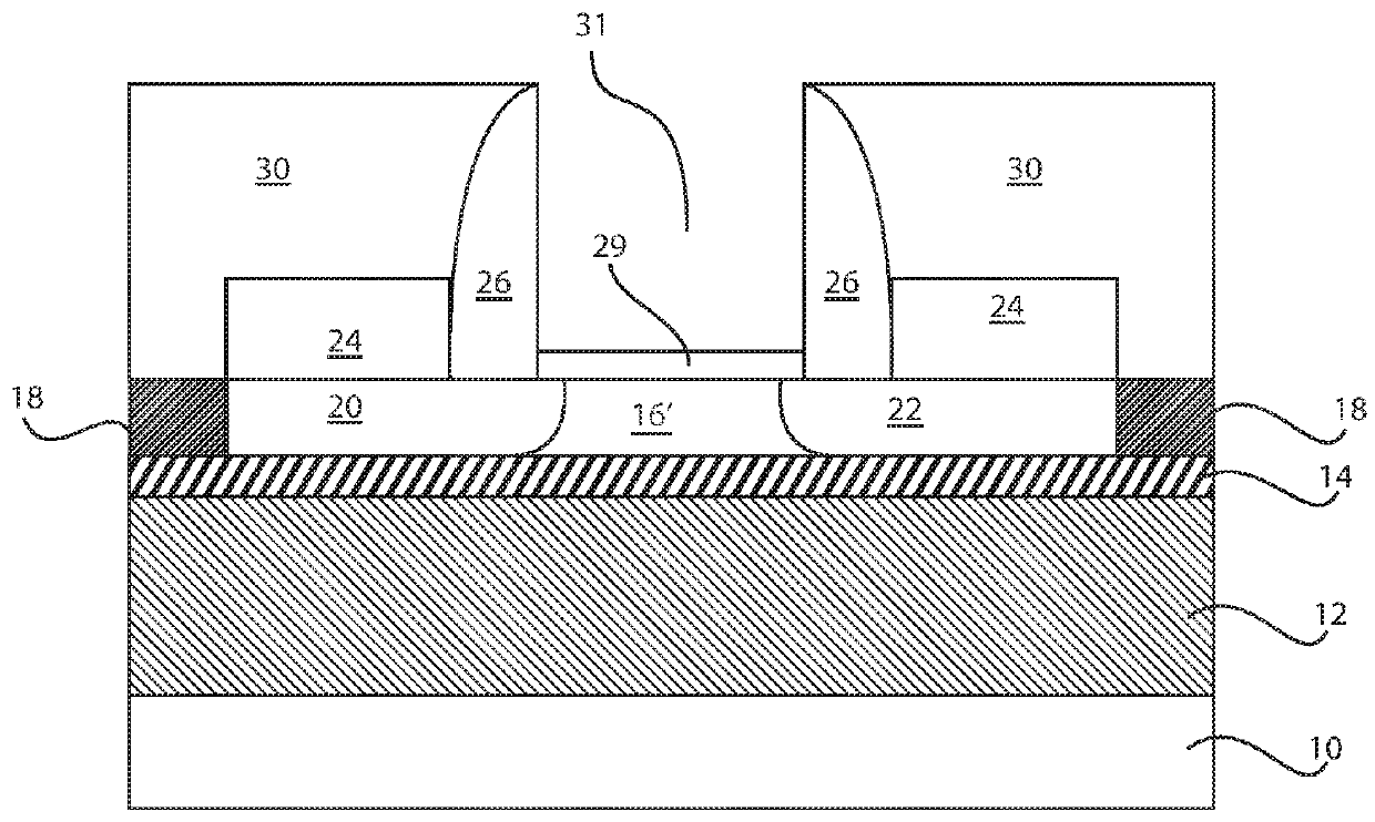
[0021]Embodiments of the present invention relate generally to the formation of a semiconductor structure for reducing parasitic back gate capacitance. The formation includes forming a bilayer buried insulator over a semiconductor substrate, forming an extremely thin silicon-on-insulator (ETSOI) over the bilayer buried insulator, forming a dummy gate over an ETSOI channel, and forming a source / drain next to the dummy gate, the source / drain defining a raised source / drain region. The method further includes depositing a dielectric material over the raised source / drain, removing the dummy gate to define a recess, implanting a species within a first layer of the bilayer buried insulator, and depositing a gate dielectric and a conducting material within the recess defined by the removal of the dummy gate. The method further includes removing the semiconductor substrate, removing the implanted species, etching a portion of the first layer of the bilayer buried insulator to expose a surfac...


PUM


Abstract

A method is presented for forming a semiconductor structure. The method includes forming a bilayer buried insulator over a substrate, forming an extremely thin silicon-on-insulator (ETSOI) over the bilayer buried insulator, forming a dummy gate, and forming a source / drain next to the dummy gate, the source / drain defining a raised source / drain region. The method further includes depositing a dielectric material over the raised source / drain regions, removing the dummy gate to define a recess, implanting a species within a first layer of the bilayer buried insulator, and depositing a gate dielectric and a conducting material within the recess. The method further includes removing the substrate, etching the implanted portion of the first layer of the bilayer buried insulator to expose a surface of a second layer of the bilayer buried insulator, and forming a back gate over the exposed second layer, the back gate self-aligned to the ETSOI channel.

Description

BACKGROUNDTechnical Field[0001]The present invention relates generally to semiconductor devices, and more specifically, to a fully-depleted silicon-on-insulator (FDSOI) device for reducing parasitic back gate capacitance.Description of the Related Art[0002]As the size of metal oxide semiconductor field effect transistors (MOSFETs) and other devices decreases, the dimensions of source / drain regions, channel regions, and gate electrodes of the devices, also decreases. The design of ever-smaller planar transistors with short channel lengths makes it necessary to provide very shallow source / drain junctions. Shallow junctions are needed to avoid lateral diffusion of implanted dopants into the channel, since such diffusion disadvantageously contributes to leakage currents and poor breakdown performance. Shallow source / drain junctions, with a thickness of about 30 nm to 100 nm, are generally required for acceptable performance in short channel devices. Silicon-on-insulator (SOI) technology...

Claims


Application Information

Patent Timeline
Patent Type & Authority Applications(United States)
IPC IPC(8): H01L29/417H01L23/535H01L29/06H01L21/265H01L21/768H01L21/762H01L29/66H01L21/306
CPCH01L29/41783H01L23/535H01L29/0649H01L21/30604H01L21/76895H01L21/76243H01L29/66545H01L21/265H01L29/4966H01L29/517H01L29/66484H01L29/7831H01L29/7834H01L21/02532H01L21/0262H01L21/76898H01L21/02634
Inventor CHENG, KANGGUODIVAKARUNI, RAMACHANDRA
Owner IBM CORP
Why Eureka
Try Eureka