Two-sided semiconductor-on-insulator structures and methods of manufacturing the same

a semiconductor and substrate technology, applied in the field of semiconductor devices, can solve the problems of increasing the boundary area between the two types of semiconductor devices, not using block masks, and not optimizing the stress of shallow trench isolation

Active Publication Date: 2008-07-31
TAIWAN SEMICON MFG CO LTD
View PDF9 Cites 266 Cited by
  • Summary
  • Abstract
  • Description
  • Claims
  • Application Information

AI Technical Summary

Benefits of technology

[0018]The semiconductor structure according to the present invention may further comprise an alignment structure that allows alignment of the semiconductor structure both with the top semiconductor layer on the upside of the buried insulator layer and with the bottom semiconductor layer on the upside of the buried insulator layer.

Problems solved by technology

For example, the stress of shallow trench isolation cannot be simultaneously optimized for both p-type devices and n-type devices since an optimal stress for a p-type metal-oxide-semiconductor field effect transistor (MOSFET) is compressive, while an optimal stress for an n-type MOSFET is tensile.
Furthermore, requirements for inter-well isolation also increase the boundary area between the two types of semiconductor devices.
Use of block masks not only increases the process complexity and cost, but also reduces the packing density due to the requirement for boundary areas between the two groups of devices.

Method used


Image

  • Two-sided semiconductor-on-insulator structures and methods of manufacturing the same
  • Two-sided semiconductor-on-insulator structures and methods of manufacturing the same
  • Two-sided semiconductor-on-insulator structures and methods of manufacturing the same

Examples


Embodiment Construction

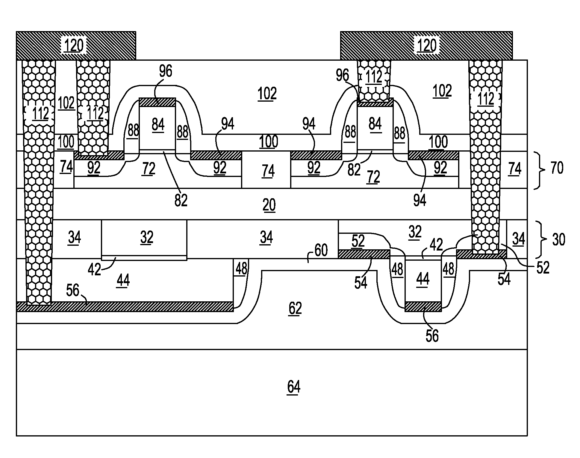
[0040]As stated above, the present invention relates to a semiconductor structure and methods of manufacturing the same, in which first type semiconductor devices are formed on one side of a buried insulator layer and second type semiconductor devices are formed on the other side of the buried insulator layer, which is now described in detail with accompanying figures.

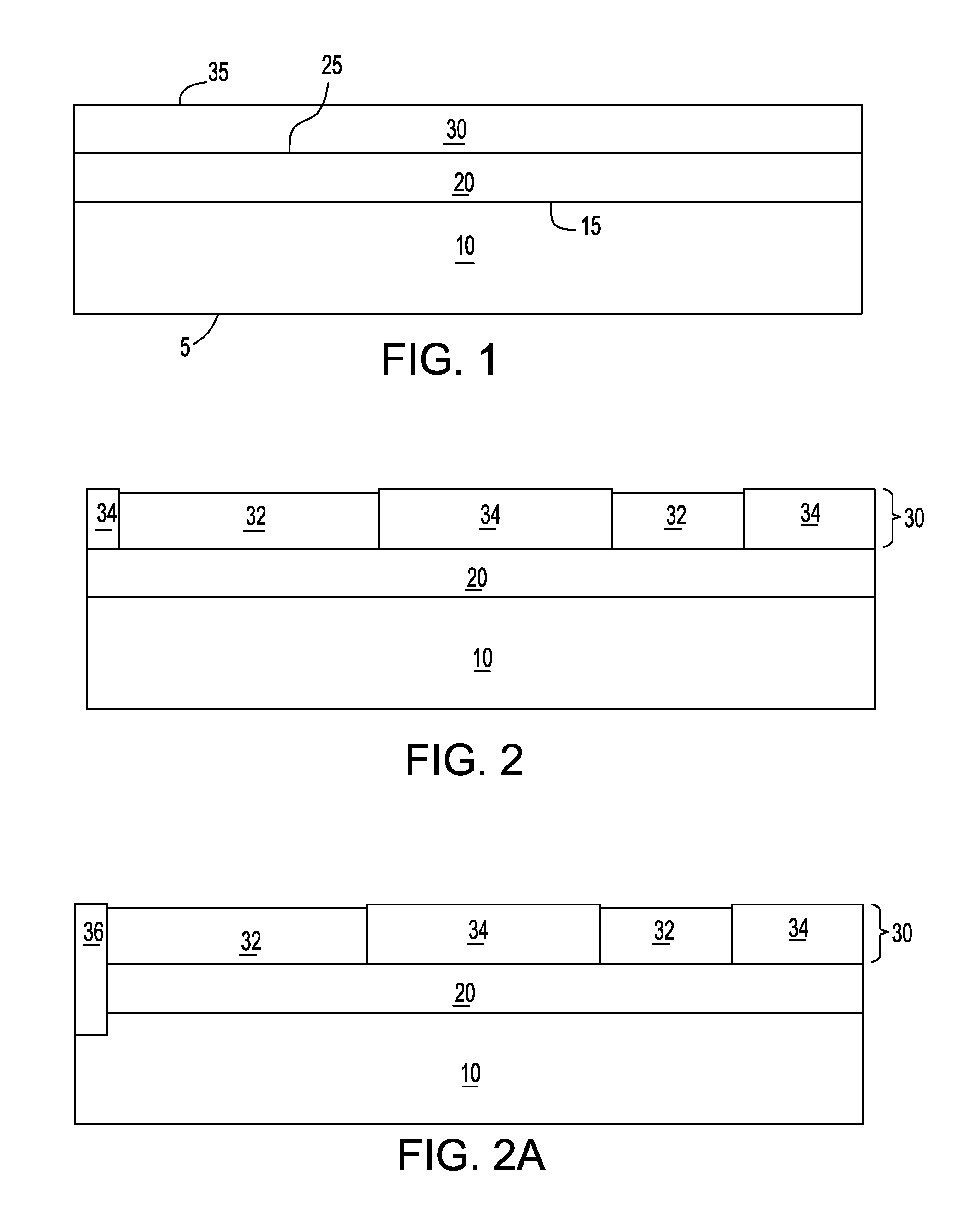
[0041]Referring to FIG. 1, a semiconductor-on-insulator (SOI) substrate is provided. The SOI substrate comprises a carrier substrate 10, a buried insulator layer 20, and a first semiconductor layer 30. Since the SOI substrate is later flipped upside down, the first semiconductor layer 30 is physically located beneath the buried insulator layer 20 in the final structure. For this reason, the first interface 25 between the buried insulator layer 20 and the first semiconductor layer 30 is herein referred to as a “bottom surface” of the buried insulator layer 20. For a similar reason, the second interface 15 between the bu...


PUM


Abstract

Both sides of a semiconductor-on-insulator substrate are utilized to form MOSFET structures. After forming first type devices on a first semiconductor layer, a handle wafer is bonded to the top of a first middle-of-line dielectric layer. A lower portion of a carrier substrate is then removed to expose a second semiconductor layer and to form second type devices thereupon. Conductive vias may be formed through the buried insulator layer to electrically connect the first type devices and the second type devices. Use of block masks is minimized since each side of the buried insulator has only one type of devices. Two levels of devices are present in the structure and boundary areas between different types of devices are reduced or eliminated, thereby increasing packing density of devices. The same alignment marks may be used to align the wafer either front side up or back side up.

Description

FIELD OF THE INVENTION[0001]The present invention relates to semiconductor devices, and particularly to semiconductor structures having semiconductor devices on both sides of a semiconductor-on-insulator substrate and methods of fabricating the same.BACKGROUND OF THE INVENTION[0002]Conventional complementary metal oxide semiconductor (CMOS) integrated circuits comprise p-type devices and n-type devices formed on the same level in a semiconductor substrate, i.e., the various components of p-type devices are coplanar with the corresponding components of the n-type devices. Some of the processing steps are common to both the p-type devices and the n-type devices, but many steps are not common and thus need to be performed separately by masking the area for one type of device while processing the other type of device. For example, the p-type and n-type devices require different well implantation, different gate polysilicon implantation, and different source and drain implantation.[0003]...

Claims


Application Information

Patent Timeline
Patent Type & Authority Applications(United States)
IPC IPC(8): H01L27/12H01L21/84H01L21/8238
CPCH01L21/84H01L27/1203H01L27/0694H01L23/481H01L23/485
Inventor DYER, THOMAS W.YANG, HAINING S.
Owner TAIWAN SEMICON MFG CO LTD
Why Eureka
Try Eureka