All-around MOSFET gate and methods of manufacture thereof

a technology of mosfet gate and mosfet channel, which is applied in the direction of transistors, semiconductor devices, electrical appliances, etc., can solve the problems of wasting space, wasting space, and wasting effort in developing efficient fabrication methods, and achieve the effect of prolonging the duration of the contact etch process

Inactive Publication Date: 2005-01-06
MINDSPEED TECH INC
View PDF13 Cites 245 Cited by
  • Summary
  • Abstract
  • Description
  • Claims
  • Application Information

AI Technical Summary

Benefits of technology

[0010] The present invention comprises a method of fabricating a metal oxide semiconductor field effect transistor (MOSFET) that supports an arbitrarily wide channel and that has a gate structure that completely surrounds the channel. The invention therefore addresses the problems associated with prior art gate-all-around MOSFETs and related technologies.
[0011] The method of the present invention, according to one variation thereof, comprises oxidizing a first surface of a silicon wafer. A void then is created in the oxide to form a gate region that, eventually, will form the “bottom” part of an all-around gate. To construct the gate, the void is partially filled with gate dielectric, and the remaining portion of the void is filled with gate material. The first surface of the wafer then is bonded to a substrate, and material is removed from a surface of the wafer opposite the first surface to expose a separation plane. The construction not removed then is “flipped over,” and the separation plane surface is processed to create a field effect transistor having a gate aligned to the gate material in the void. The gate of the field effect transistor then is electrically connected to the gate material contained in the void.
[0012] In one variation of the present method, the first surface is bonded to a substrate by blanketing the first surface with a dielectric layer and adhering the dielectric layer to the substrate. In another variation of the method, the first surface is separated from the wafer by implanting the first surface of the wafer with hydrogen and cleaving the wafer proximate to the hydrogen implantation boundary. Alternatively, according to another variation of the method, the first surface is separated from the wafer by grinding the wafer from a surface opposite the first surface. Partially filling the void in the oxide with gate dielectric, according to one variation of the present method, comprises growing a dielectric material in the void. According to another variation of the method, filling the void with gate dielectric comprises depositing a dielectric material in the void. In yet another variation of the method, filling the remaining portion of the void with gate material comprises depositing a layer of gate material over the first surface and removing excess gat

Problems solved by technology

Consequently, considerable effort has been expended to develop efficient fabrication methods for creating MOSFETs that possess various desirable properties that reach beyond the gross requirements of low cost, small size, high speed, and low power consumption.
One issue in MOSFET design concerns the geometry of the gate that normally comprises one of the electrical inputs to a MOSFET.
In practice, the geometry of the gate and channel can become quite complicated.
One problem with the gate-all-around MOSFET concerns the fabrication method used to implement the portion of the gate that underlies the channel.
Such a long etch step would mean that the smallest transistor would have a large size consistent with the long etch, thereby wasting space and leading to larger chip size than necessary.
Additionally, if the bridge is approximately the same width as the thickness of the underlying insulating layer, the etch will completely remove the insulating

Method used


Image

  • All-around MOSFET gate and methods of manufacture thereof
  • All-around MOSFET gate and methods of manufacture thereof
  • All-around MOSFET gate and methods of manufacture thereof

Examples


Embodiment Construction

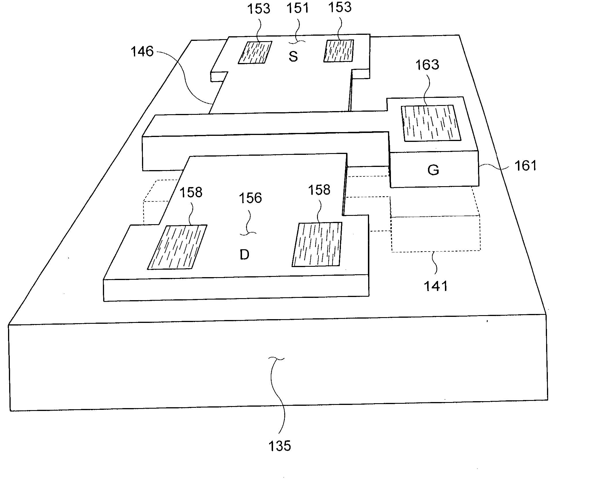
[0028] The present invention comprises a method of fabricating a metal oxide semiconductor field effect transistor (MOSFET) that supports an arbitrarily wide channel and that has a gate structure that completely surrounds the channel. The invention therefore addresses the problems associated with prior art gate-all-around MOSFETs and related technologies. The method represents an enhancement to traditional silicon-on-insulator (SOI) circuit fabrication techniques wherein processing of bonded SOI wafers currently is performed on a thin transferred wafer slice after bonding to a “handle” wafer. The invention teaches that processing can be done on the “back” of the thin slice to be transferred before it is separated from its parent wafer. The invention provides a useful method of building an all-around gate MOSFET and way of constructing very wide MOSFETs on the same circuit.

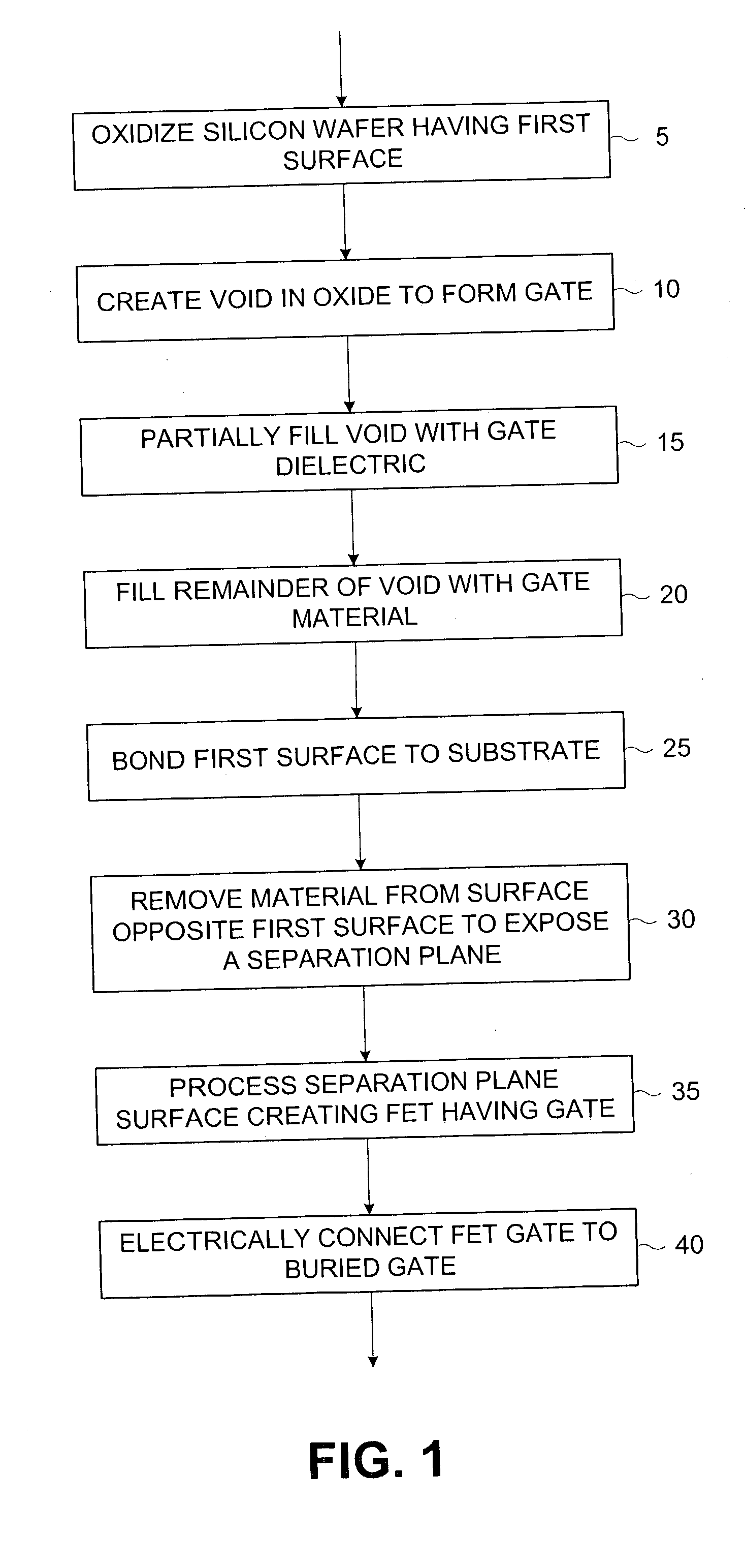
[0029]FIG. 1 is a flow diagram that describes one example variation of a method for preparing a channel gate ac...


PUM


Abstract

Metal oxide field effect transistor having a channel and a gate that surrounds the channel on four sides. Method of manufacture of the transistor includes processing the back of a silicon wafer to form a buried gate that is electrically connected to the gate of a conventional field effect transistor to form an all-around structure.

Description

FIELD OF THE INVENTION [0001] The present invention relates generally to metal oxide semiconductor field effect transistors, and more particularly to field effect transistors having a gate that surrounds a channel region. BACKGROUND OF THE INVENTION [0002] Metal oxide semiconductor field effect transistors (MOSFETs) have been called the most common devices ever manufactured by man. Considering that each of the millions of integrated circuits that are manufactured every day around the world contains millions of MOSFETs, this statement probably is true. MOSFETs are, without doubt, the most common elements in today's very large scale integrated (VLSI) circuits. Consequently, considerable effort has been expended to develop efficient fabrication methods for creating MOSFETs that possess various desirable properties that reach beyond the gross requirements of low cost, small size, high speed, and low power consumption. [0003] Use of bonded semiconductor-on-insulator (SOI) wafers has been...

Claims


Application Information

Patent Timeline
IPC IPC(8): H01L21/336H01L29/423H01L29/786
CPCH01L29/42384H01L29/785H01L29/66795H01L29/42392
Inventor JONES, A. BROOKE
Owner MINDSPEED TECH INC
Why Eureka
Try Eureka