Methods to fabricate MOSFET devices using selective deposition process

a selective deposition and mosfet technology, applied in the direction of semiconductor devices, chemical vapor deposition coatings, coatings, etc., can solve the problems of increasing series resistance, increasing series resistance, and challenging production of ultra shallow source/drain junctions

Active Publication Date: 2005-04-14
APPLIED MATERIALS INC
View PDF21 Cites 224 Cited by
  • Summary
  • Abstract
  • Description
  • Claims
  • Application Information

AI Technical Summary

Benefits of technology

[0015] In another embodiment, a method for forming a silicon-based material on a substrate surface is provided which includes exposing the substrate surface to a process gas, depositing a first silicon-based layer with a crystalline lattice on the substrate surface containing less than 3 atomic percent (at %) carbon in interstitial sites of the crystalline lattice, and annealing the first silicon-based layer to incorporate at least a portion of the less than 3 at % carbon in substitutional sites of the crystalline lattice.
[0016] In another embodiment, a method for depositing a silicon-containing material on a substrate surface is provided which includes depositing a first silicon-containing layer on the substrate surface with a first germanium concentration of about 24 at % or less, depositing on the first silicon-containing layer a second silicon-containing layer wherein a second germanium concentration of about 25 at % or more of the second silicon-containing layer, and depositing on the second silicon-containing layer a third silicon-containing layer containing a third germanium concentration less than about 5 at % of the third silicon-containing layer.
[0017] In another embodiment, a method for depositing a silicon-containing material on a substrate surface is provided which includes depositing a first silicon-containing layer on the substrate surface with a first germanium concentration of about 15 at % or more. The method further provides depositing on the first silicon-containing layer a second silicon-containing layer wherein a second germanium concentration of about 15 at % or less, exposing the substrate surface to air to form a native oxide layer, removing the native oxide layer to expose the second silicon-containing layer, and depositing a third silicon-containing layer on the second silicon-containing layer.

Problems solved by technology

As smaller transistors are manufactured, ultra shallow source / drain junctions are becoming more challenging to produce.
On the other hand, the ultra shallow source / drain junction inevitably results in increased series resistance.
Also, junction consumption during silicide formation increases the series resistance even further.
Although SiGe-epitaxial deposition is suitable for small dimensions, this approach does not readily prepare doped SiGe, since the dopants react with HCl.
The process development of heavily boron doped (e.g., higher than 5×1019 cm−3) selective SiGe-epitaxy is a much more complicated task because boron doping makes the process window for selective deposition narrow.

Method used


Image

  • Methods to fabricate MOSFET devices using selective deposition process
  • Methods to fabricate MOSFET devices using selective deposition process
  • Methods to fabricate MOSFET devices using selective deposition process

Examples


examples

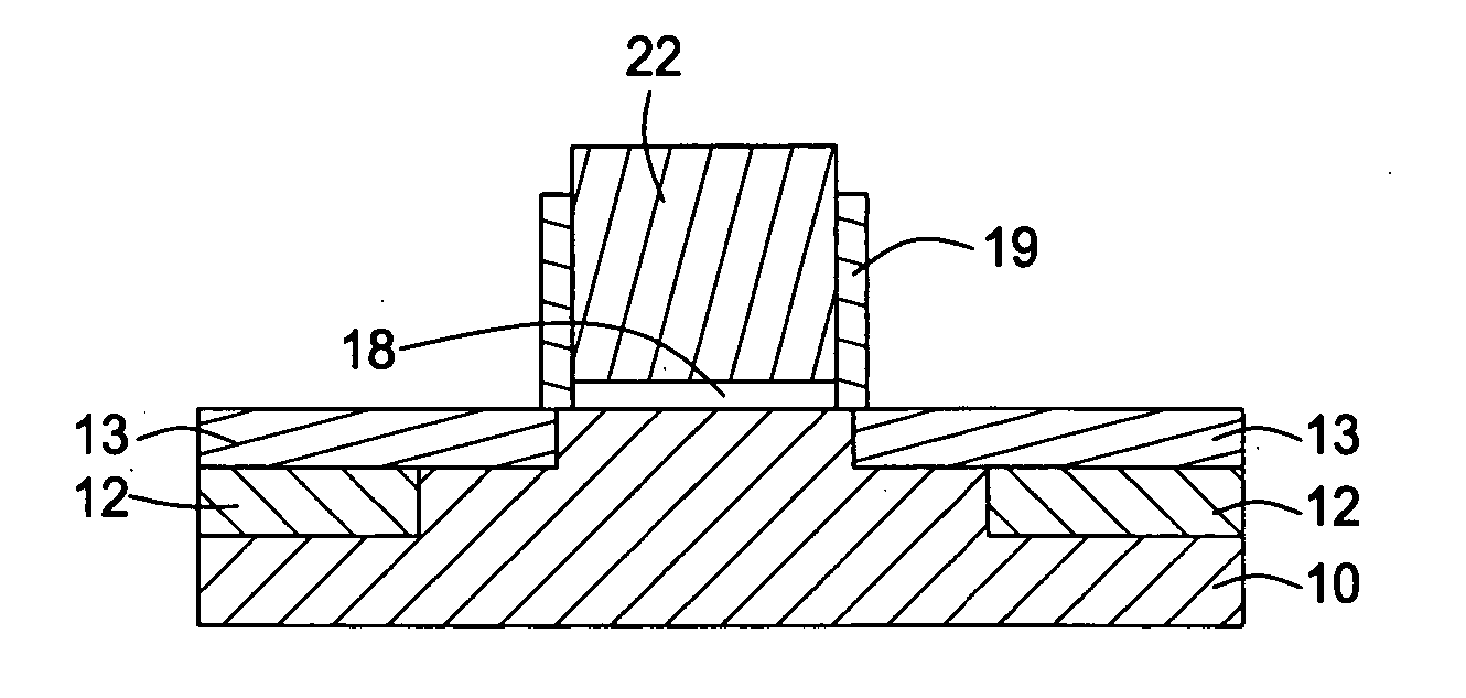
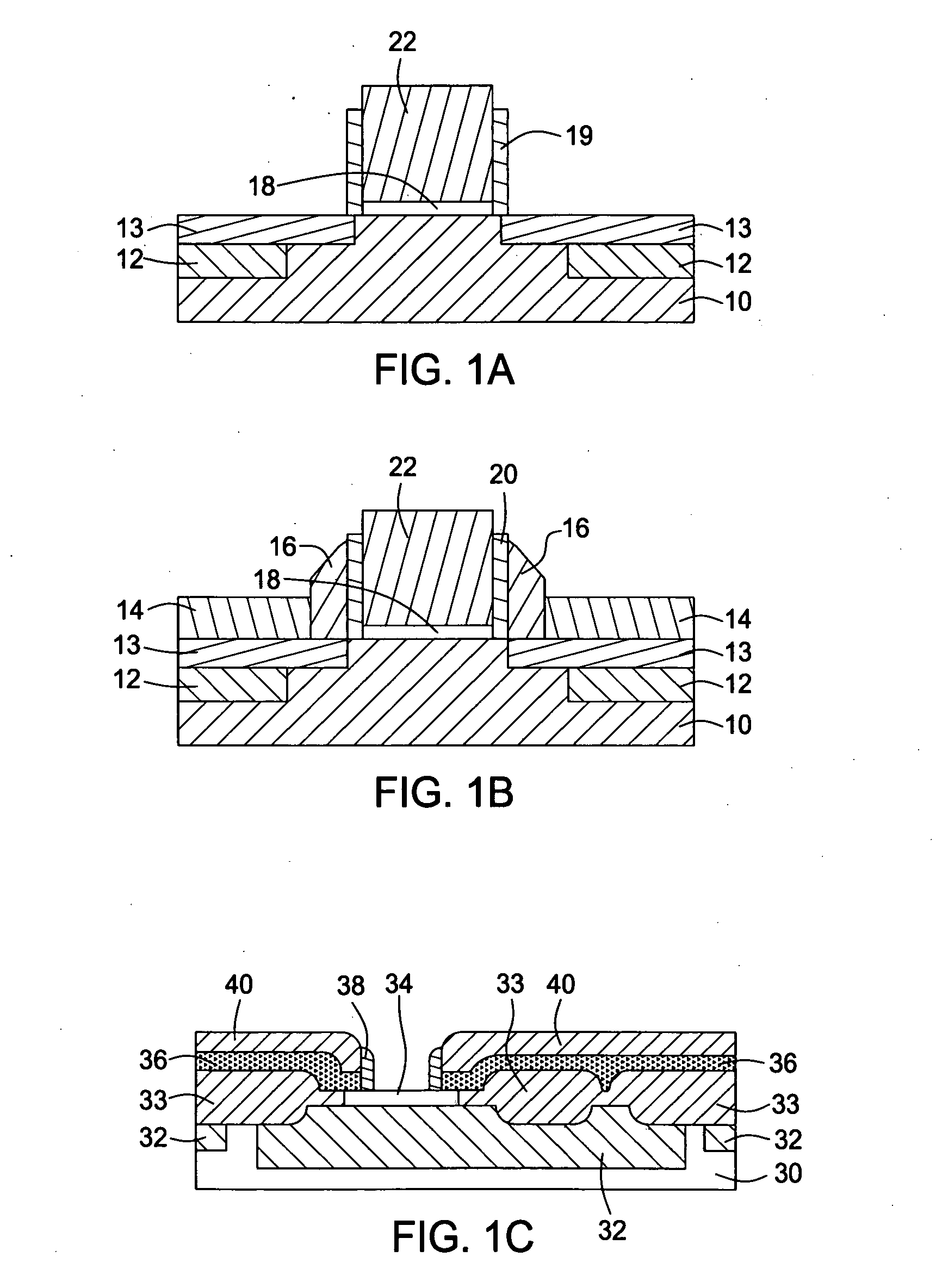
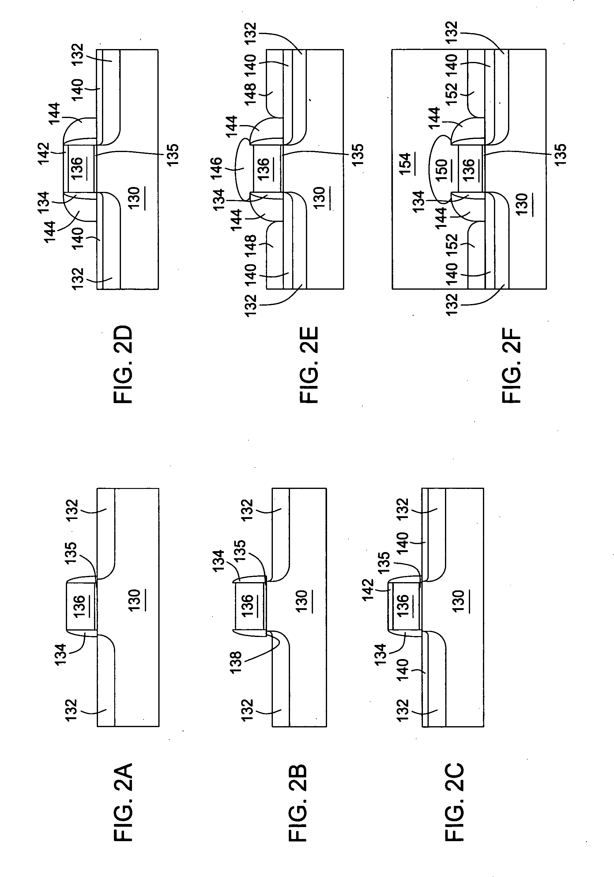
[0071] Example 1 SiGe / Si stack: A substrate, Si, (e.g., 300 mm OD) was employed to investigate selective, monocrystalline film growth by CVD. A dielectric feature existed on the surface of the wafer. The wafer was prepared by subjecting to a 1% HF dip for 45 seconds. The wafer was loaded into the deposition chamber (Epi Centura® chamber) and baked in a hydrogen atmosphere at 800° C. for 60 seconds to remove native oxide. A flow of carrier gas, hydrogen, was directed towards the substrate and the source compounds were added to the carrier flow. Dichlorosilane (100 sccm) and germane (1% GeH4 in H2, 280 sccm) were added to the chamber at 3 Torr and 725° C. Also, hydrogen chloride (190 sccm) and diborane (1% in H2, 150 sccm) were delivered to the chamber. The substrate was maintained at 0.725° C. Deposition was conducted for about 5 minutes to form a 500 Å SiGe film with a germanium concentration of about 20 at % and the boron concentration of about 1.0×1020 cm3. The substrate was remov...


PUM

PropertyMeasurementUnit
pressureaaaaaaaaaa
temperatureaaaaaaaaaa

Abstract

In one embodiment, a method for fabricating a silicon-based device on a substrate surface is provided which includes depositing a first silicon-containing layer by exposing the substrate surface to a first process gas comprising Cl2SiH2, a germanium source, a first etchant and a carrier gas and depositing a second silicon-containing layer by exposing the first silicon-containing layer to a second process gas comprising SiH4 and a second etchant. In another embodiment, a method for depositing a silicon-containing material on a substrate surface is provided which includes depositing a first silicon-containing layer on the substrate surface with a first germanium concentration of about 15 at % or more. The method further provides depositing on the first silicon-containing layer a second silicon-containing layer wherein a second germanium concentration of about 15 at % or less, exposing the substrate surface to air to form a native oxide layer, removing the native oxide layer to expose the second silicon-containing layer, and depositing a third silicon-containing layer on the second silicon-containing layer. In another embodiment, a method for depositing a silicon-containing material on a substrate surface is provided which includes depositing epitaxially a first silicon-containing layer on the substrate surface with a first lattice strain, and depositing epitaxially on the first silicon-containing layer a second silicon-containing layer with a second lattice strain greater than the first lattice strain.

Description

CROSS-REFERENCE TO RELATED APPLICATION [0001] This application is a continuation-in-part of U.S. patent application Ser. No. 10 / 683,937, filed Oct. 10, 2003, which is herein incorporated by reference.BACKGROUND OF THE INVENTION [0002] 1. Field of the Invention [0003] Embodiments of the invention generally relate to the field of semiconductor manufacturing processes and devices, more particular, to methods of depositing silicon-containing films forming semiconductor devices. [0004] 2. Description of the Related Art [0005] As smaller transistors are manufactured, ultra shallow source / drain junctions are becoming more challenging to produce. According to the International Technology Roadmap for Semiconductors (ITRS), junction depth is required to be less than 30 nm for sub-100 nm CMOS (complementary metal-oxide semiconductor) devices. Recently, selective SiGe epitaxy has become a useful material to deposit during formation of elevated source / drain and source / drain extension features. S...

Claims


Application Information

Patent Timeline
Patent Type & Authority Applications(United States)
IPC IPC(8): H01L21/20H01L21/205H01L21/28H01L21/331H01L21/336H01L21/8238
CPCH01L21/0245H01L29/7848H01L21/02529H01L21/02532H01L21/02576H01L21/02579H01L21/0262H01L21/02636H01L21/28044H01L21/28114H01L21/823807H01L21/823814H01L29/165H01L29/66242H01L29/665H01L29/66545H01L29/6656H01L29/66628H01L29/66636H01L29/78H01L29/7834H01L21/0251
Inventor SAMOILOV, ARKADII V.KIM, YIHWANSANCHEZ, ERROLDALIDA, NICHOLAS C.
Owner APPLIED MATERIALS INC
Why Eureka
Try Eureka