Method and structure for a 1T-RAM bit cell and macro

a micro-cell and micro-cell technology, applied in the field of manufacturing of semiconductor devices, can solve the problems of reducing the size of conventional mos transistors, affecting the performance of conventional planar mos transistors, or errors,

Inactive Publication Date: 2008-09-16
TAIWAN SEMICON MFG CO LTD
View PDF16 Cites 253 Cited by
  • Summary
  • Abstract
  • Description
  • Claims
  • Application Information

AI Technical Summary

Benefits of technology

[0053]In another preferred embodiment of the invention, the MIM capacitor is formed using a technique to create a roughened, granular bottom electrode over a layer of irradiated metal, the dielectric and the top electrode material are conformally deposited using atomic layer deposition (ALD) techniques and the roughened surfaces between the plates and the dielectric result in increased capacitance in the same area.

Problems solved by technology

However, as the size of conventional MOS transistors is reduced with the scaling reductions of the overall process technology, conventional planar MOS transistor structures start to become less desirable.
As the channel width of a MOSFET transistor is reduced certain “short channel” effects may occur where the source and drain regions remain electrically coupled even when the device is off, these effects can result in undesirable or even unacceptable performance, or errors.

Method used


Image

  • Method and structure for a 1T-RAM bit cell and macro
  • Method and structure for a 1T-RAM bit cell and macro
  • Method and structure for a 1T-RAM bit cell and macro

Examples


Embodiment Construction

[0077]The operation and fabrication of the presently preferred embodiments are discussed in detail below. However, the embodiments and examples described are not the only applications or uses contemplated for the invention. The specific embodiments discussed are merely illustrative of specific ways to make and use the invention, and do not limit the scope of the invention. The figures are for illustrative purposes and are not drawn to scale.

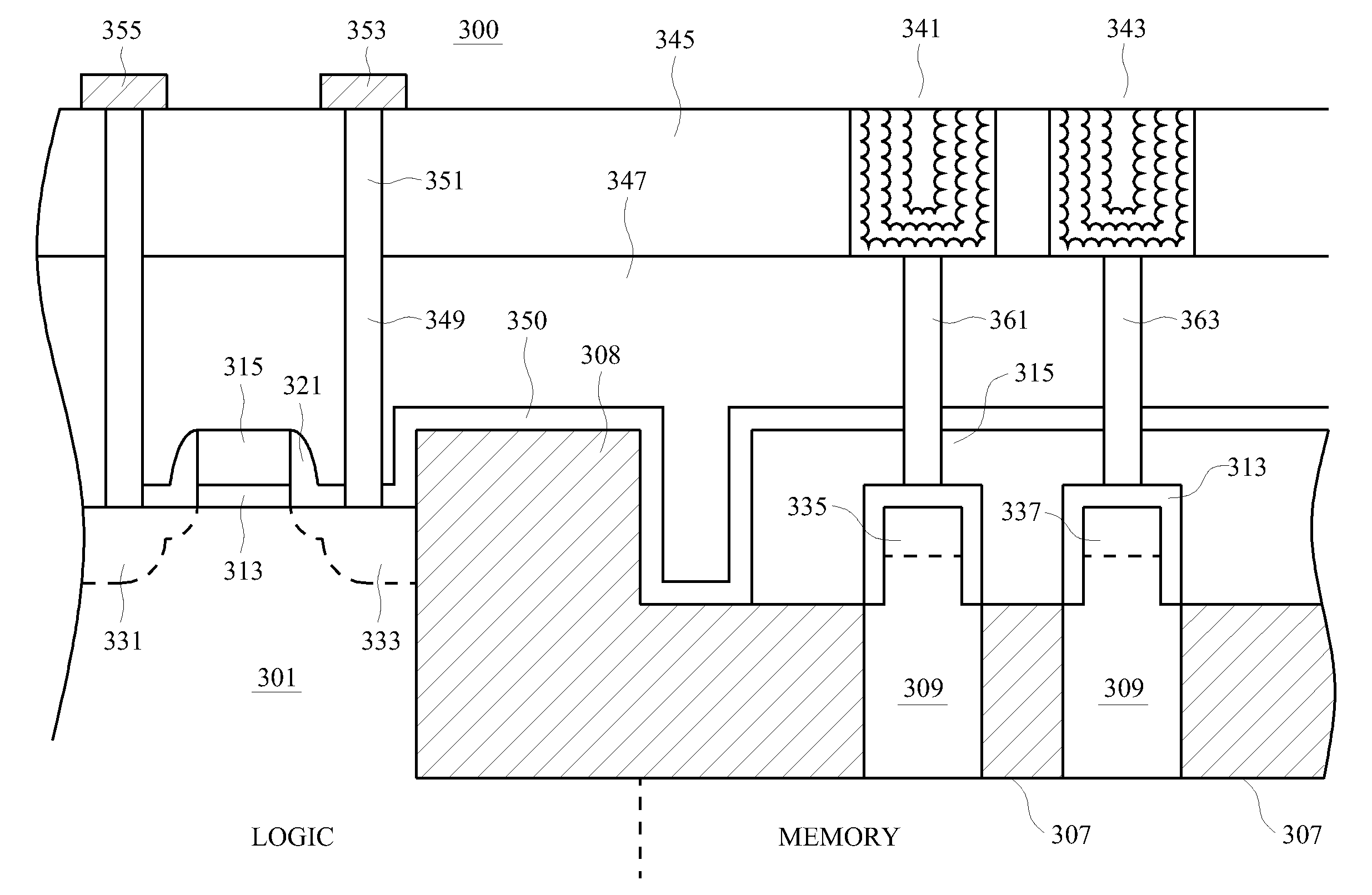
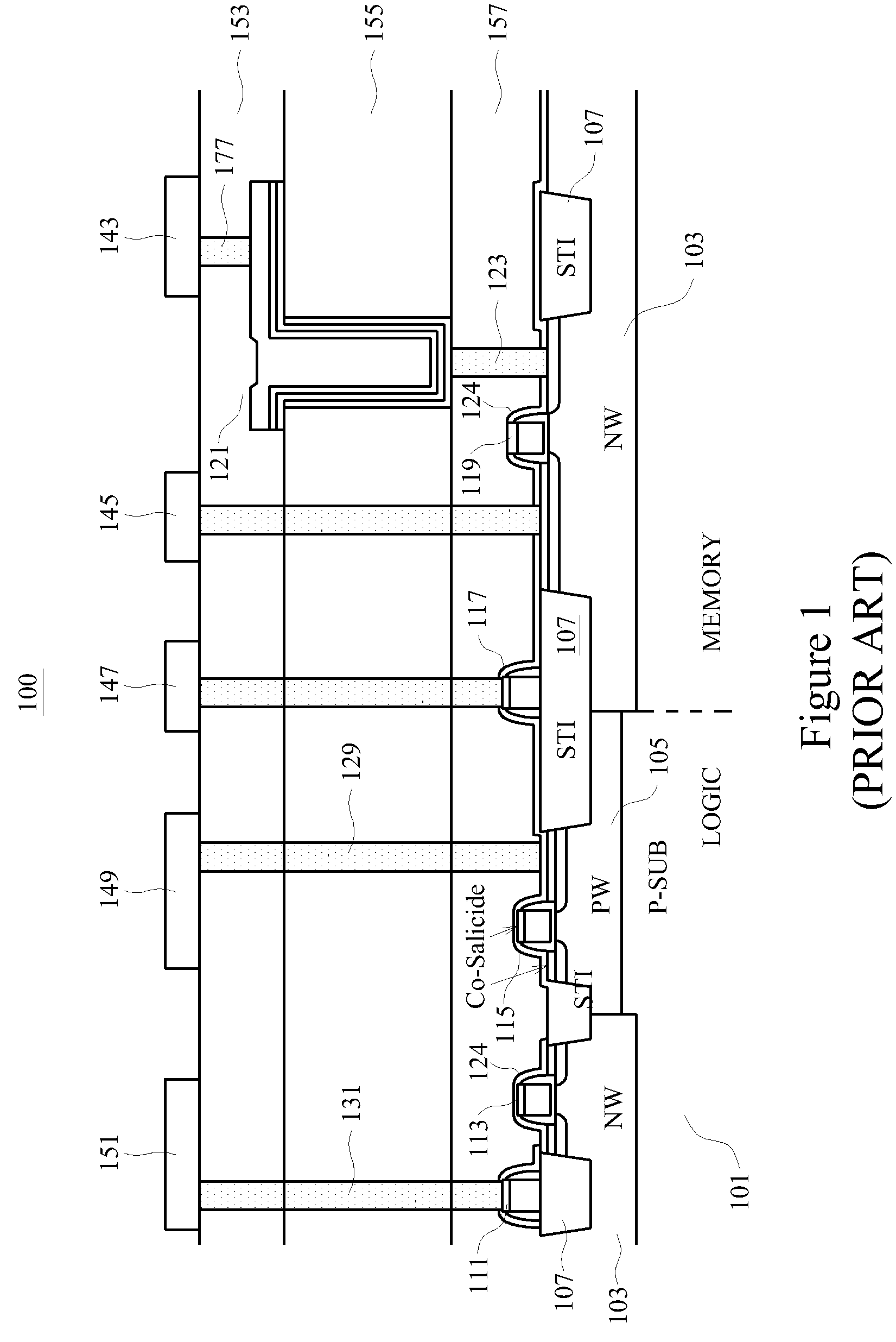
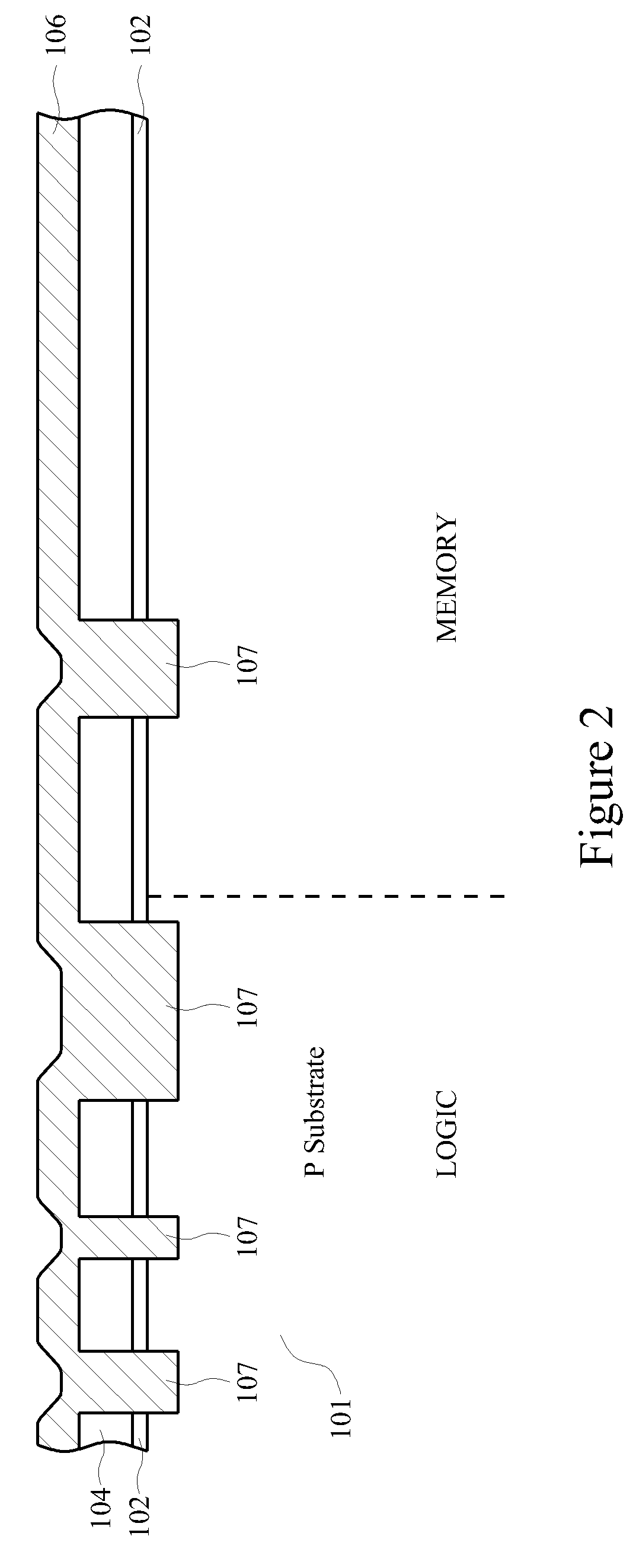
[0078]The present invention will be described with respect to preferred embodiments, some of which are described in terms of an example application for an embedded DRAM device incorporating a finFET access transistor in the memory array area. The embedded DRAM may be incorporated into any number of integrated circuits including microprocessors, digital and analog signal processors, microcontrollers, ASICs of any kind, and other integrated circuits which use storage as part of the circuitry, particularly, integrated circuits which process data. Em...


PUM


Abstract

A one transistor (1T-RAM) bit cell and method for manufacture are provided. A metal-insulator-metal (MIM) capacitor structure and method of manufacturing it in an integrated process that includes a finFET transistor for the 1T-RAM bit cell is provided. In some embodiments, the finFET transistor and MIM capacitor are formed in a memory region and an asymmetric processing method is disclosed, which allows planar MOSFET transistors to be formed in another region of a single device. In some embodiments, the 1T-RAM cell and additional transistors may be combined to form a macro cell, multiple macro cells may form an integrated circuit. The MIM capacitors may include nanoparticles or nanostructures to increase the effective capacitance. The finFET transistors may be formed over an insulator. The MIM capacitors may be formed in interlevel insulator layers above the substrate. The process provided to manufacture the structure may advantageously use conventional photomasks.

Description

TECHNICAL FIELD[0001]The present invention and the various embodiments described generally relate to the fabrication of semiconductor devices, and more particularly to fabricating integrated devices which incorporate planar MOS transistors, one or more MIM (metal-insulator-metal) storage capacitors, and / or one or more finFET transistors to form a memory storage cell, such as a one transistor bit cell, and macro cells including one or more of said memory storage cells.BACKGROUND[0002]In the semiconductor art, it is desirable to add RAM storage onto an integrated circuit which also comprises other circuitry, for example, for microprocessor circuits (MPUs,) microcontroller circuits (MCUs), digital signal processors (DSPs), RF or filter circuitry which uses stored data or parameteric information, analog-to-digital converters and the like, or other advanced circuitry which requires data or program storage to be rapidly accessible by programmable or logic circuitry. In the prior art this ...

Claims


Application Information

Patent Timeline
Patent Type & Authority Patents(United States)
IPC IPC(8): H01L27/108H01L27/01H01L27/12H01L29/76H01L29/94
CPCH01L28/82H01L27/10897H01L27/10823H01L27/10826H01L27/10879H01L27/10894H01L27/1211H01L29/66795H01L29/785H01L21/845H10B12/34H10B12/36H10B12/056H10B12/50H10B12/09
Inventor LIU, SHENG-DACHEN, HUNG-WEICHANG, CHANG-YUNXUAN, ZHONG TANGHSU, JU-WANG
Owner TAIWAN SEMICON MFG CO LTD
Why Eureka
Try Eureka