Method of fabricating printed circuit board having embedded multi-layer passive devices

a printed circuit board and passive device technology, applied in the direction of electrical apparatus contruction details, conductive pattern formation, association of printed circuit non-printed electric components, etc., can solve the problems of not reaching the desired product requirements and the actual usability has decreased, and achieve the effect of increasing capacitan

Inactive Publication Date: 2007-11-13
SAMSUNG ELECTRO MECHANICS CO LTD
View PDF15 Cites 124 Cited by
  • Summary
  • Abstract
  • Description
  • Claims
  • Application Information

AI Technical Summary

Benefits of technology

[0074]According to the method of the present invention, the advantage of the multi-layer structure can be sufficiently exhibited to obtain capacitance density greatly affecting decoupling to a desired level.

Problems solved by technology

However, such conventional techniques suffer because the capacitance is very low, thus decreasing actual usability.
To solve the problems, although attempts to use a component material having high capacitance have been made, they have not yet reached desired product requirements.

Method used


Image

  • Method of fabricating printed circuit board having embedded multi-layer passive devices
  • Method of fabricating printed circuit board having embedded multi-layer passive devices
  • Method of fabricating printed circuit board having embedded multi-layer passive devices

Examples


Embodiment Construction

[0024]Hereinafter, embodiments of the present invention are described, with reference to the appended drawings.

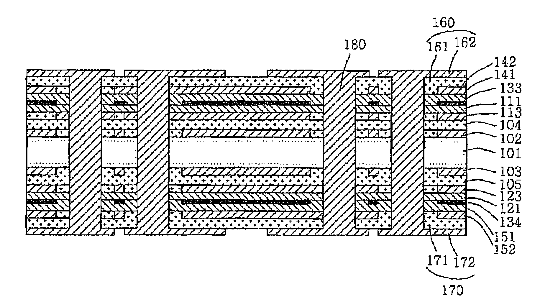
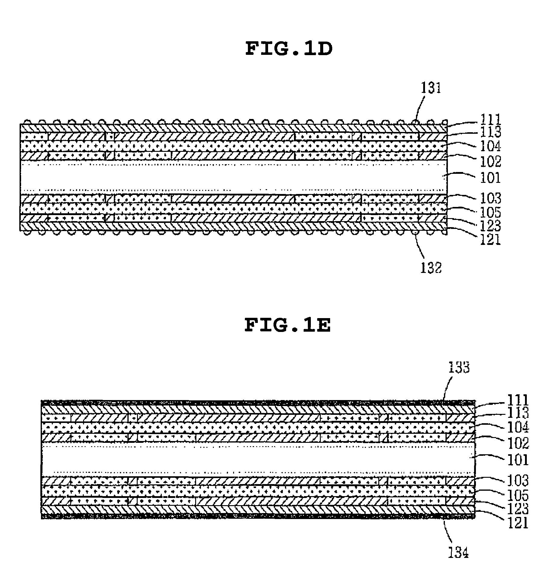
[0025]FIGS. 1A to 1J sequentially illustrate a process of fabricating a PCB including an embedded multi-layer capacitor, according to an embodiment of the present invention.

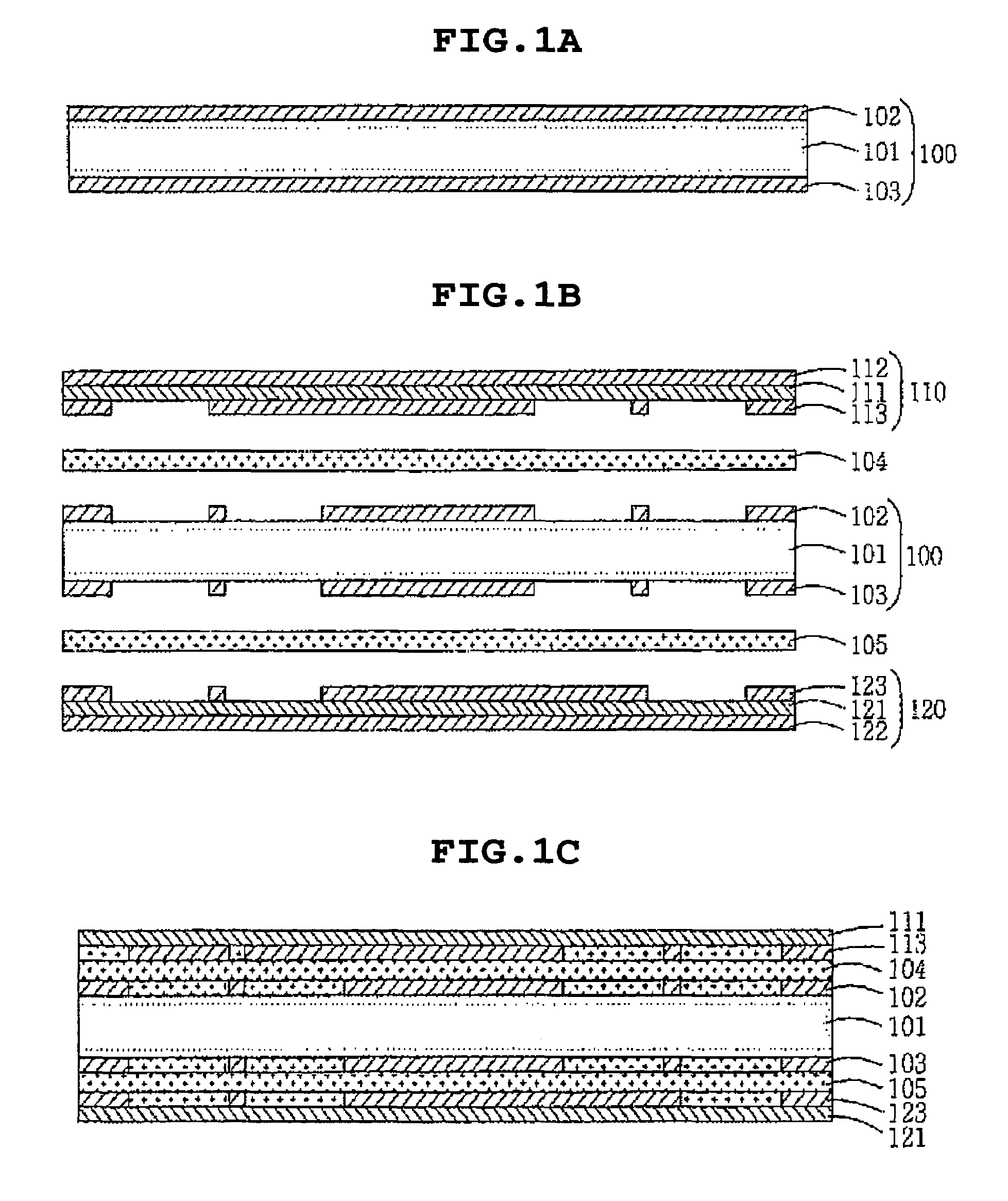
[0026]As shown in FIG. 1A, a copper foil 102 of a base substrate 100 constituting a core layer undergoes an imaging process, to form a circuit pattern.

[0027]A copper clad laminate (CCL) used as the base substrate 100 is classified into glass / epoxy CCLs, heat resistant resin CCLs, paper / phenol CCLs, high frequency CCLs, flexible CCLs, complex CCLs, etc., depending on its uses. Of these CCLs, a glass / epoxy CCL 100 including an insulating resin layer 101 coated with copper foils 102, 103 is preferably used, in order to fabricate a double-sided PCB or a multi-layered PCB.

[0028]After a dry film (not shown) is applied on the base substrate 100, the dry film is exposed and developed, using an art work film havi...


PUM

PropertyMeasurementUnit
thicknessaaaaaaaaaa
thicknessaaaaaaaaaa
dielectric constantaaaaaaaaaa

Abstract

The present invention relates to a method of fabricating a printed circuit board having embedded multi-layer passive devices, and particularly, to a method of fabricating a printed circuit board having an embedded multi-layer capacitor, in which a capacitor is formed to have multiple layers in the PCB to increase capacitance.

Description

INCORPORATION BY REFERENCE[0001]The present application claims priority under 35 U.S.C. §119 to Korean Patent Application No. 10-2005-0020572 filed on Mar. 11, 2005. The content of the application is incorporated herein by reference in its entirety.BACKGROUND OF THE INVENTION[0002]1. Field of the Invention[0003]The present invention relates, generally, to a method of fabricating a printed circuit board (PCB) having embedded multi-layer passive devices, and more particularly, to a method of fabricating a PCB having an embedded multi-layer capacitor, in which a capacitor is formed to have multiple layers in the PCB to increase capacitance.[0004]2. Description of the Related Art[0005]Although discrete chip resistors or discrete chip capacitors have been generally mounted on almost all PCBs to date, PCBs in which passive devices, such as resistors or capacitors are embedded have recently been developed.[0006]In techniques of fabricating PCBs including embedded passive devices, the passi...

Claims


Application Information

Patent Timeline
Patent Type & Authority Patents(United States)
IPC IPC(8): H01K3/10
CPCH05K1/162H05K3/4652H05K3/4661Y10T29/49155H05K3/381H05K3/429H05K3/4626H05K3/4655H05K2201/0209H05K2201/0358H05K2201/09309H05K2203/1152Y10T29/49165Y10T29/4913Y10T29/49126H05K3/025H05K3/46
Inventor SOHN, SEUNG HYUNCHUNG, YUL KYOJIN, HYUN JUPARK, EUN TAE
Owner SAMSUNG ELECTRO MECHANICS CO LTD
Why Eureka
Try Eureka