Transistor structure with thick recessed source/drain structures and fabrication process of same

a transistor and source/drain technology, applied in the field of semiconductor processing, can solve the problems of difficult to improve various performance of semiconductor devices using bulk wafers, low resistance contact from source/drain regions to channels in thin soi films, and degrade performance and/or reliability, etc., to achieve the effect of increasing gate-to-s/d capacitance, reducing s/d resistance, and increasing s/d conductivity

Inactive Publication Date: 2005-03-22
IBM CORP
View PDF44 Cites 151 Cited by
  • Summary
  • Abstract
  • Description
  • Claims
  • Application Information

AI Technical Summary

Benefits of technology

In contrast to previous generations of field effect transistors (FETs), the present invention provides improved transistor structures with thick recessed source / drain (S / D) structures without any complex device engineering. The thick recessed S / D structures decrease S / D resistance (i.e., increase S / D conductivity) without increasing gate-to-S / D capacitance, thereby increasing device operation.

Problems solved by technology

Unfortunately, increased device density in FETs often results in degradation of performance and / or reliability.
Additionally, with increased device density in FETs, it is difficult to improve various performances of semiconductor devices using a bulk wafer.
However, a good, low resistant contact from the source / drain regions to the channel in a thin SOI film are difficult to make.
Conventional methods attempt to solve this problem by raising the source / drain (S / D) regions on either side of the transistor resulting in low S / D resistance.
Therefore, this increase in gate-to-S / D capacitance leads to a decrease in device performance.
This is one of the limiting factors for SOI device performance.

Method used


Image

  • Transistor structure with thick recessed source/drain structures and fabrication process of same
  • Transistor structure with thick recessed source/drain structures and fabrication process of same
  • Transistor structure with thick recessed source/drain structures and fabrication process of same

Examples


Embodiment Construction

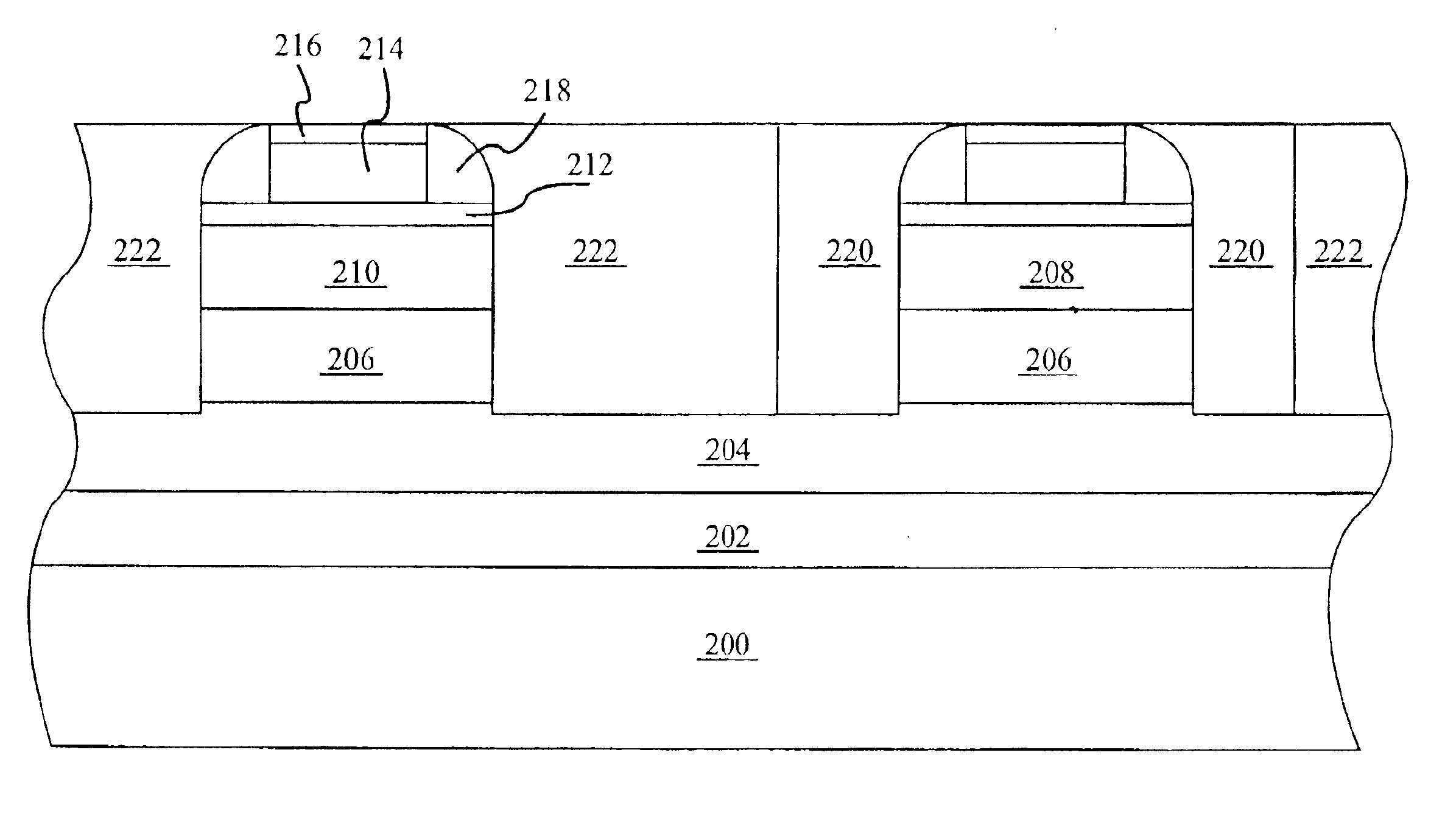
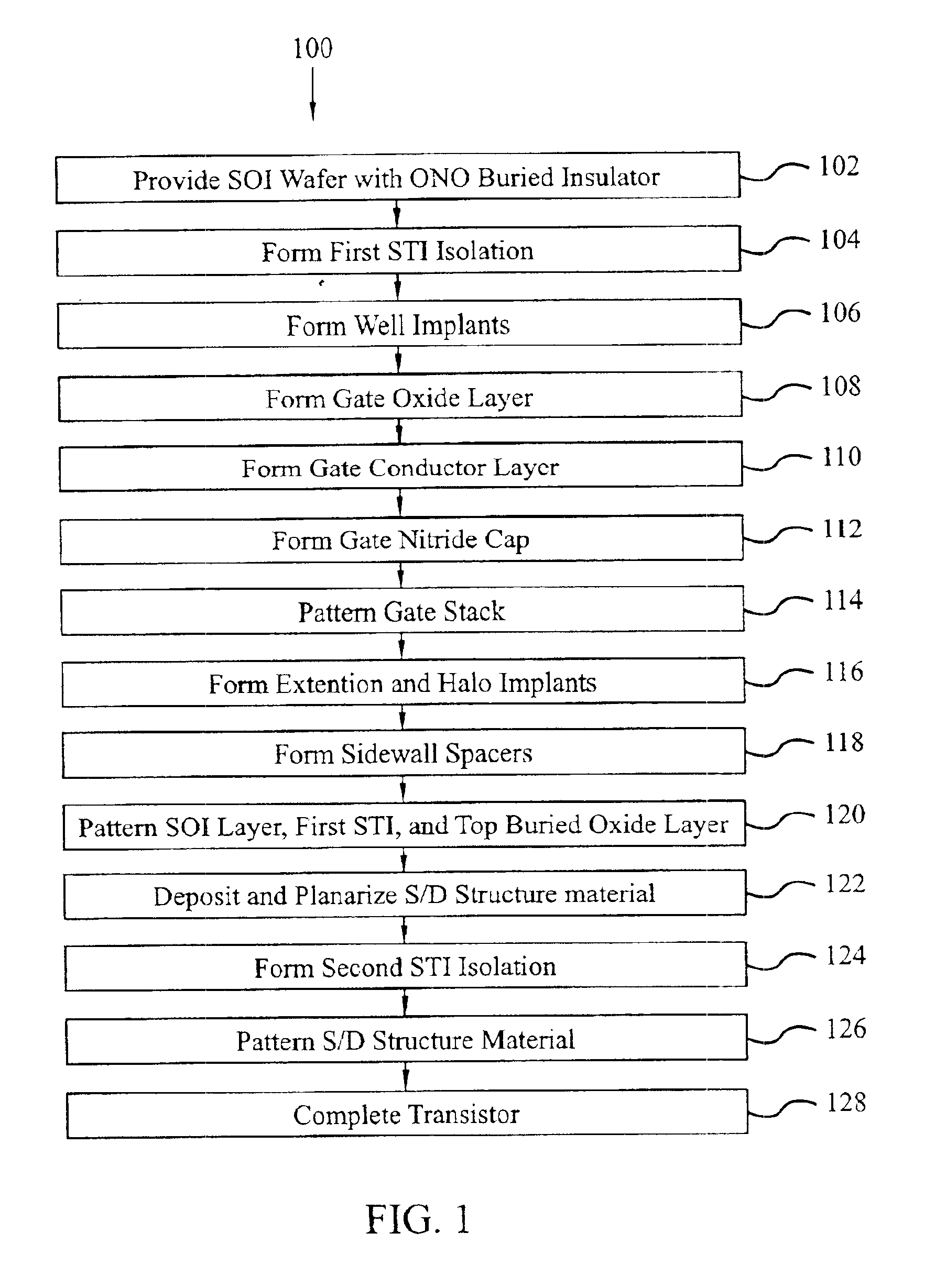
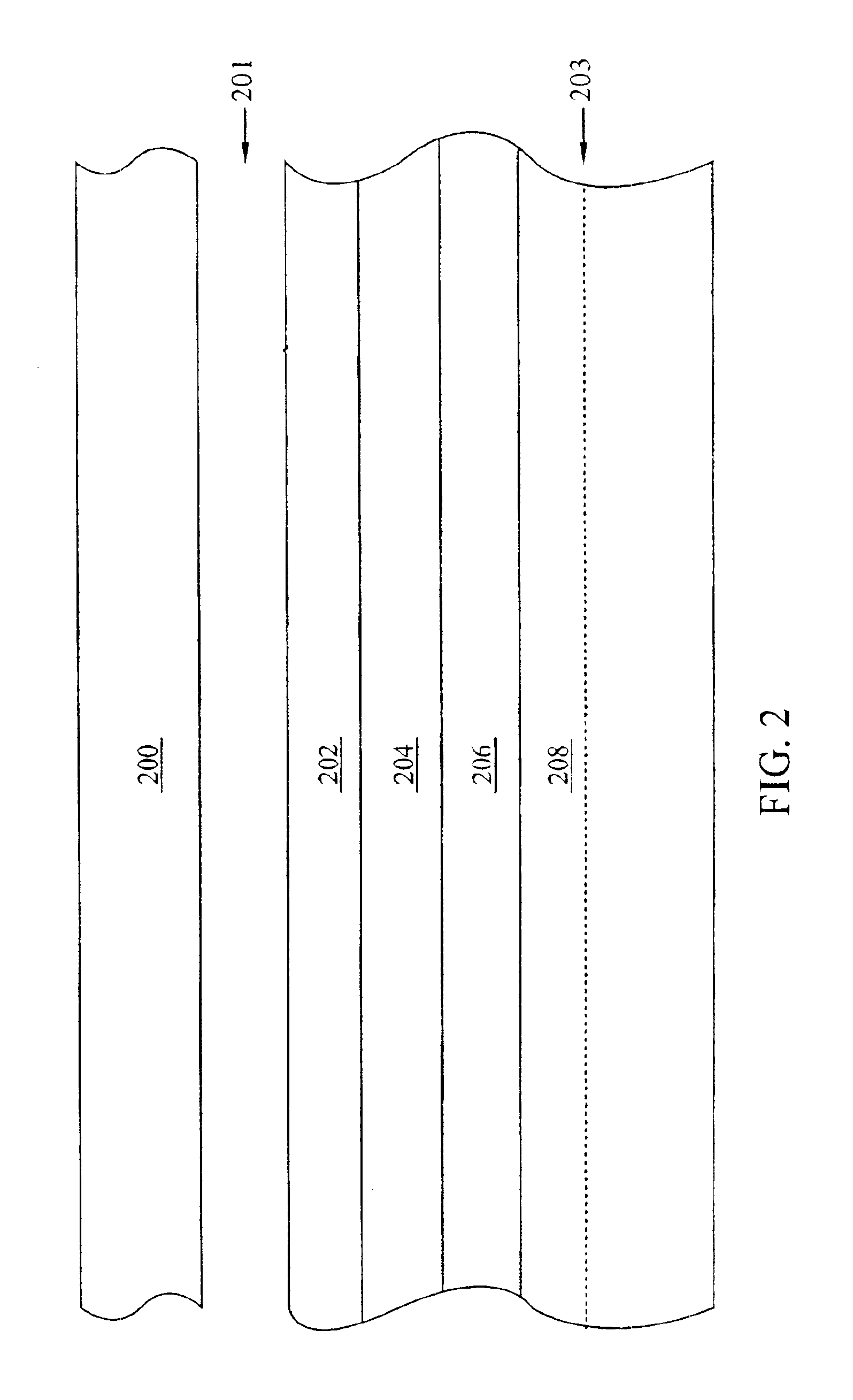
The present invention may be readily adapted to a variety of methods of fabricating a transistor structure with thick recessed source / drain (S / D) structures that decrease S / D resistance without increasing gate-to-S / D capacitance, thereby increasing device operation. The present invention relates to any type of field effect transistor (FET), such as, for example, metal oxide semiconductor (MOS) FETs, complimentary metal oxide semiconductor (CMOS) FETs, n-channel metal oxide semiconductor (NMOS) FETs, p-channel metal oxide semiconductor (PMOS) FETs, and the like. Moreover, it will be understood by one of ordinary skill in the art that the invention is not limited to the specific structures illustrated in the drawings or to the specific steps detailed herein. It will also be understood that the invention is not limited to use of any specific dopant types provided that the dopant types selected for the various components are consistent with the intended electrical operation of the devic...


PUM


Abstract

An improved transistor structure that decreases source/drain (S/D) resistance without increasing gate-to-S/D capacitance, thereby increasing device operation. S/D structures are formed into recesses formed on a semiconductor wafer through a semiconductor layer and a first layer of a buried insulator having at least two layers. A body is formed from the semiconductor layer situated between the recesses, and the body comprises a top body surface and a bottom body surface that define a body thickness. Top portions of the S/D structures are within and abut the body thickness. An improved method for forming the improved transistor structure is also described and comprises: forming recesses through a semiconductor layer and a first layer of a buried insulator so that a body is situated between the recesses; and forming S/D structures into the recesses so that top portions of the S/D structures are within and abut a body thickness.

Description

BACKGROUND OF THE INVENTION1. Technical FieldThe present invention relates generally to the field of semiconductor processing and, more specifically, to a fabrication process for a transistor structure with thick recessed source / drain (S / D) structures.2. Background ArtThe need to remain cost and performance competitive in the production of semiconductor devices has caused continually increasing device density in integrated circuits. To facilitate the increase in device density, new technologies are constantly needed to allow the feature size of these semiconductor devices to be reduced.The push for ever increasing device densities is particularly strong in CMOS technologies, such as the in the design and fabrication of field effect transistors (FETs). FETs are the basic electrical devices of today's integrated circuits and are used in almost all types of integrated circuit design (i.e., microprocessors, memory, etc.). FETs may be formed on conventional substrates such as a silicon w...

Claims


Application Information

Patent Timeline
Patent Type & Authority Patents(United States)
IPC IPC(8): H01L21/70H01L29/786H01L29/417H01L21/02H01L29/423H01L29/66H01L27/12H01L21/336H01L21/84H01L29/40
CPCH01L21/84H01L27/1203H01L29/41733H01L29/785H01L29/66772H01L29/66795H01L29/42384
Inventor BRYANT, ANDRESJAFFE, MARK D.
Owner IBM CORP
Why Eureka
Try Eureka