Semiconductor device and method for manufacturing the same

a technology of semiconductors and semiconductors, applied in the direction of instruments, optics, transistors, etc., can solve the problems of increased power consumption, electric signal leakage between wirings, delay in transmission of signals, etc., and achieve the effect of improving reliability, favorable electric characteristics, and high reliability

Active Publication Date: 2011-02-03
SEMICON ENERGY LAB CO LTD
View PDF100 Cites 146 Cited by
  • Summary
  • Abstract
  • Description
  • Claims
  • Application Information

AI Technical Summary

Benefits of technology

[0037]Accordingly, it is possible to manufacture and provide a semiconductor device including a highly reliable thin film transistor having favorable electric characteristics.
[0038]Note that by forming the high-resistance drain region in the oxide semiconductor layer overlapping with the drain electrode layer, the reliability when a driver circuit is formed can be improved. Specifically, by forming the high-resistance drain region, a structure can be obtained in which conductivity can be varied from the drain electrode layer to the high-resistance drain region and the channel formation region. Therefore, in the case where the thin film transistor operates with the drain electrode layer connected to a wiring for supplying a high power supply potential VDD, the high-resistance drain region serves as a buffer and a high electric field is not applied locally even if a high electric field is applied between the gate electrode layer and the drain electrode layer, so that the withstand voltage of the transistor can be improved.
[0039]In addition, the high-resistance drain region is formed in the oxide semiconductor layer overlapping with the drain electrode layer (and the source electrode layer), so that reduction in leakage current can be achieved in the channel formation region in forming the driver circuit. In particular, when the high-resistance

Problems solved by technology

In addition, when the parasitic capacitance is large, delay of transmission of a signal may occur.
Further, increase in the parasitic capacitance causes a cross talk phenomenon in which an electric signal leaks between wirings or increase in

Method used


Image

  • Semiconductor device and method for manufacturing the same
  • Semiconductor device and method for manufacturing the same
  • Semiconductor device and method for manufacturing the same

Examples


embodiment 1

[0087]In this embodiment, one embodiment of a semiconductor device and a method for manufacturing the semiconductor device will be described with reference to FIGS. 1A to 1C, FIGS. 2A to 2E, FIGS. 3A and 3B, and FIGS. 4A1, 4A2, 4B1, and 4B2.

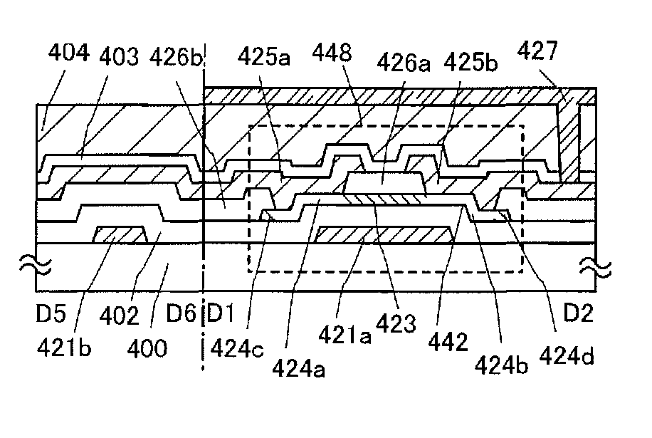
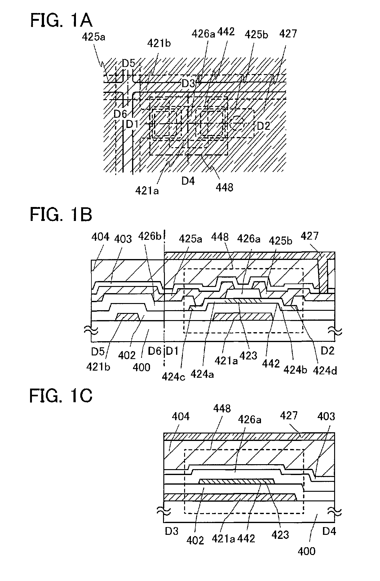
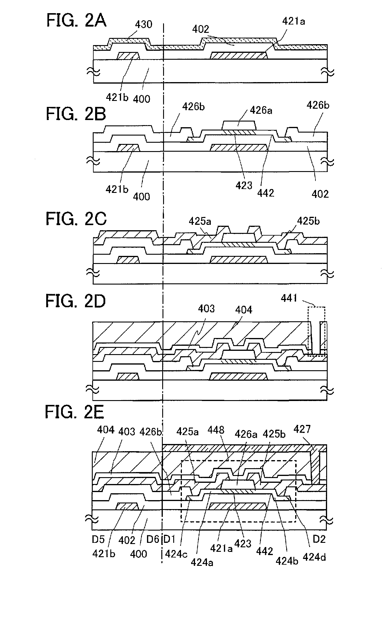
[0088]FIG. 1A is a plan view of a channel protective thin film transistor 448 provided in a pixel, and FIG. 1B is a cross-sectional view taken along line D1-D2 and D5-D6 of FIG. 1A. FIG. 1C is a cross-sectional view taken along line D3-D4. Note that FIG. 2E is the same as FIG. 1B.

[0089]The thin film transistor 448 provided in the pixel is a channel protective (also referred to as channel-stop) thin film transistor, which includes, over a substrate 400 having an insulating surface, a gate electrode layer 421a, a gate insulating layer 402, an oxide semiconductor layer 442 including a channel formation region 423, an oxide insulating layer 426a functioning as a channel protective layer, a source electrode layer 425a, and a drain electrode layer 425b...

embodiment 2

[0139]In this embodiment, description is provided of an example in which an active matrix liquid crystal display device is manufactured by using the thin film transistor described in Embodiment 1 to form a pixel portion and a driver circuit over one substrate.

[0140]FIG. 3A illustrates an example of a cross-sectional structure of the active matrix substrate.

[0141]Although the thin film transistor in the pixel portion and the wiring intersection are described in Embodiment 1, the thin film transistor in the driver circuit, the storage capacitor, the gate wiring, and a terminal portion of the source wiring are also described in this embodiment as well as the thin film transistor and the wiring intersection. The capacitor, the gate wiring, and the terminal portion of the source wiring can be formed in the same process as the manufacturing process described in Embodiment 1. Further, in a portion serving as a display region of the pixel portion, the gate wiring, the source wiring, and a c...

embodiment 3

[0180]In this embodiment, an example of a structure of a terminal portion provided over the same substrate as the thin film transistor is described. Although an example of the terminal portion of the source wiring is described in Embodiment 2, a terminal portion of the source wiring which is different from the terminal portion described in Embodiment 2 and a terminal portion of the gate wiring are described in this embodiment. Note that in FIGS. 4A1 to 4B2, the same portions as FIGS. 3A and 3B are denoted by the same reference numerals.

[0181]FIGS. 4A1 and 4A2 respectively illustrate a cross-sectional view and a top view of the terminal portion of the gate wiring. FIG. 4A1 is a cross-sectional view taken along line C1-C2 of FIG. 4A2. In FIG. 4A1, a conductive layer 225 formed over the protective insulating layer 203 is a connection terminal electrode which functions as an input terminal. Furthermore, in the terminal portion of FIG. 4A1, a first terminal 221 formed using the same mate...


PUM


Abstract

An object is to provide a semiconductor device having a structure with which parasitic capacitance between wirings can be sufficiently reduced. An oxide insulating layer serving as a channel protective layer is formed over part of an oxide semiconductor layer overlapping with a gate electrode layer. In the same step as formation of the oxide insulating layer, an oxide insulating layer covering a peripheral portion of the oxide semiconductor layer is formed. The oxide insulating layer which covers the peripheral portion of the oxide semiconductor layer is provided to increase the distance between the gate electrode layer and a wiring layer formed above or in the periphery of the gate electrode layer, whereby parasitic capacitance is reduced.

Description

TECHNICAL FIELD[0001]The present invention relates to a semiconductor device using an oxide semiconductor and a method for manufacturing the semiconductor device.[0002]In this specification, a semiconductor device generally means a device which can function by utilizing semiconductor characteristics, and an electro-optical device such as a display device, a semiconductor circuit, and an electronic appliance are all semiconductor devices.BACKGROUND ART[0003]In recent years, a technique for forming a thin film transistor (TFT) by using a semiconductor thin film (having a thickness of approximately several nanometers to several hundred nanometers) formed over a substrate having an insulating surface has attracted attention. Thin film transistors are applied to a wide range of electronic devices such as ICs and electro-optical devices, and prompt development of thin film transistors that are to be used particularly as switching elements in image display devices is being pushed. Various ...

Claims


Application Information

Patent Timeline
IPC IPC(8): H01L29/786H01L21/34H01L29/772H01L21/84
CPCH01L27/1214H01L27/124H01L27/1225H01L29/7869H01L29/517H01L27/1248H01L29/78609G02F1/133345G02F1/1337G02F1/134309G02F1/136227G02F1/136277G02F1/1368H01L29/24
Inventor YAMAZAKI, SHUNPEIOHARA, HIROKISASAKI, TOSHINARINODA, KOSEIKUWABARA, HIDEAKI
Owner SEMICON ENERGY LAB CO LTD
Why Eureka
Try Eureka