Light-emitting device and manufacturing method thereof

a technology of light-emitting devices and manufacturing methods, which is applied in the manufacture of final products, solid-state devices, basic electric elements, etc., can solve the problems of increasing the capacity load of a thin film transistor itself and the small on/off ratio, and achieve excellent electric characteristics and high reliability.

Active Publication Date: 2011-03-17
SEMICON ENERGY LAB CO LTD
View PDF31 Cites 77 Cited by
  • Summary
  • Abstract
  • Description
  • Claims
  • Application Information

AI Technical Summary

Benefits of technology

[0061]By using an oxide semiconductor layer, a light-emitting device including a thin film transistor having excellent electric characteristics and high reliability can be realized.

Problems solved by technology

However, in the case where the channel length (L) is shortened, there is a problem of switching characteristics, for example, an on / off ratio becomes small.
In addition, when the channel width (W) is increased, there is a problem in that the capacity load of a thin film transistor itself is increased.

Method used


Image

  • Light-emitting device and manufacturing method thereof
  • Light-emitting device and manufacturing method thereof
  • Light-emitting device and manufacturing method thereof

Examples


embodiment 1

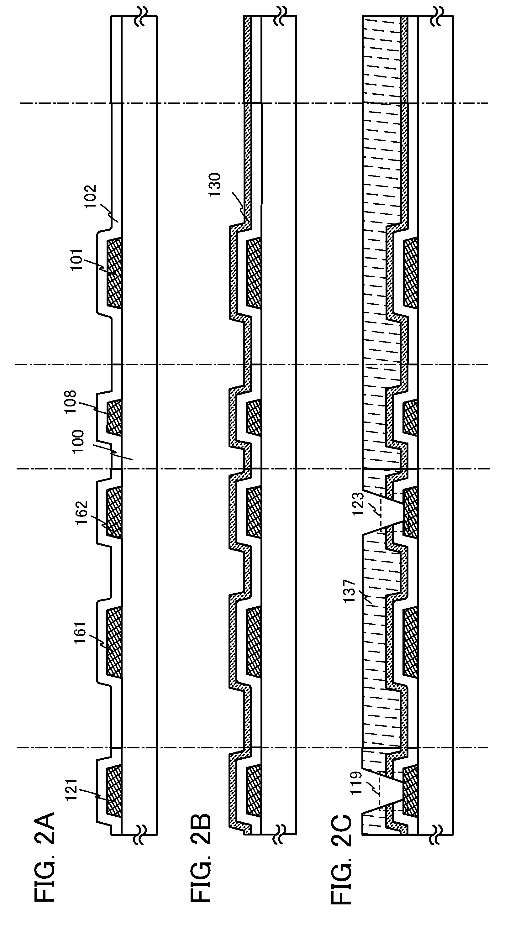
[0094]A light-emitting device including a thin film transistor and a manufacturing process thereof will be described with reference to FIG. 1, FIGS. 2A to 2C, FIGS. 3A to 3C, FIGS. 4A and 4B, FIGS. 5A and 5B, and FIGS. 11A1, 11A2, 11B1, and 11B2.

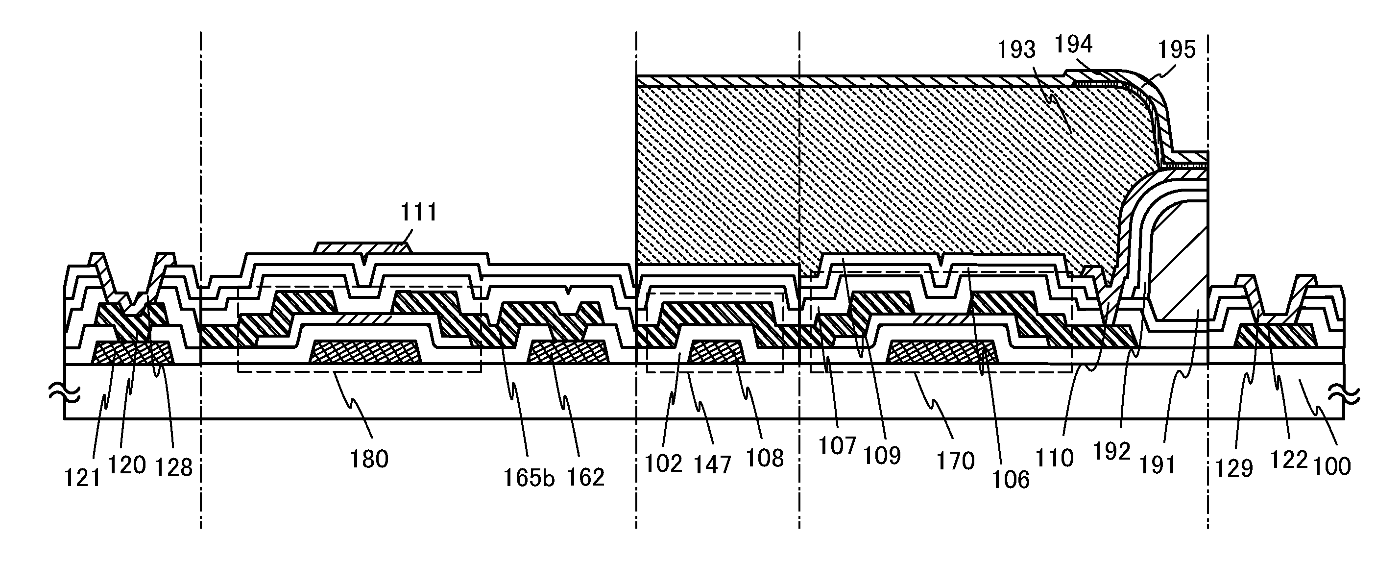
[0095]FIG. 1 shows a light-emitting device which is one mode of the present invention. The light-emitting device in FIG. 1 includes, over a flexible substrate 100, a pixel portion including a light-emitting element, a thin film transistor 170, and a capacitor 147, and a driving circuit portion including a thin film transistor 180. Further, a first terminal 121, a connection electrode 120, and a terminal electrode 128 for connection are provided in a terminal portion for a gate wiring and a second terminal 122 and a terminal electrode 129 for connection are provided in a terminal portion of a source wiring. In addition, an oxide insulating film 107 and a protective insulating layer 106 are formed over the thin film transistor 180 and the thin...

embodiment 2

[0191]In this embodiment, an example in which oxide conductive layers are provided as a source region and a drain region between the oxide semiconductor layer and the source and drain electrode layers in Embodiment 1 will be described with reference to FIGS. 6A to 6D and FIGS. 7A and 7B. Therefore, part of this embodiment can be performed in a manner similar to that of Embodiment 1; thus, repetitive description of the same portions as or portions having functions similar to those in Embodiment 1 and steps for forming such portions will be omitted. Since FIGS. 6A to 6D and FIGS. 7A and 7B are the same as FIG. 1, FIGS. 2A to 2C, FIGS. 3A to 3C, FIGS. 4A and 4B, and FIGS. 5A and 5B except for part of steps, the same portions are denoted by the same reference numerals and detailed description of the same portions is omitted.

[0192]First, the steps up to and including the step in FIG. 3B in Embodiment 1 are performed in accordance with Embodiment 1. FIG. 6A shows the same step as FIG. 3B....

embodiment 3

[0216]In this embodiment, another example in which oxide conductive layers are provided as a source region and a drain region between the oxide semiconductor layer and the source and drain electrode layers in Embodiment 1 or 2 will be described with reference to FIGS. 8A to 8D and FIGS. 9A and 9B. Therefore, part of this embodiment can be performed in a manner similar to that of Embodiment 1 or 2; thus, repetitive description of the same portions as or portions having functions similar to those in Embodiment 1 or 2 and steps for forming such portions will be omitted. Since FIGS. 8A to 8D and FIGS. 9A and 9B are the same as FIG. 1, FIGS. 2A to 2C, FIGS. 3A to 3C, FIGS. 4A and 4B, FIGS. 5A and 5B, FIGS. 6A to 6D, and FIGS. 7A and 7B except for part of steps, the same portions are denoted by the same reference numerals and detailed description of the same portions is omitted.

[0217]First, in accordance with Embodiment 1, a metal conductive film is formed over the substrate 100, and the ...


PUM


Abstract

An object of the invention is to improve the reliability of a light-emitting device. Another object of the invention is to provide flexibility to a light-emitting device having a thin film transistor using an oxide semiconductor film. A light-emitting device has, over one flexible substrate, a driving circuit portion including a thin film transistor for a driving circuit and a pixel portion including a thin film transistor for a pixel. The thin film transistor for a driving circuit and the thin film transistor for a pixel are inverted staggered thin film transistors including an oxide semiconductor layer which is in contact with a part of an oxide insulating layer.

Description

TECHNICAL FIELD[0001]The present invention relates to a light-emitting device including a layer containing an organic compound as a light-emitting layer, and a manufacturing method for the light-emitting device. For example, the present invention relates to an electronic device in which a light-emitting display device having an organic light-emitting element is mounted as a component.[0002]Note that in this specification, a semiconductor device refers to all devices that can function by utilizing semiconductor characteristics, and electro-optic devices such as light-emitting devices, semiconductor circuits, and electronic devices are all semiconductor devices.BACKGROUND ART[0003]A light-emitting element using an organic compound as a light-emitting body, which has features such as thinness, lightness, high-speed response, and DC drive at a low voltage, has been examined to be applied to a next-generation flat panel display or next-generation lighting. In particular, a display device...

Claims


Application Information

Patent Timeline
Patent Type & Authority Applications(United States)
IPC IPC(8): H01L29/22H01L33/02
CPCH01L27/12H01L51/5012H01L27/1225Y02E10/549Y02P70/50H01L29/7869H10K50/11H01L29/78606H10K59/126H10K59/131H10K59/1213H10K77/111H01L27/124H01L29/78678
Inventor EGUCHI, SHINGOOIKAWA, YOSHIAKIOKAZAKI, KENICHIMARUYAMA, HOTAKA
Owner SEMICON ENERGY LAB CO LTD
Why Eureka
Try Eureka