Semiconductor device package having buffered memory module and method thereof

a memory module and semiconductor technology, applied in the direction of semiconductor/solid-state device details, sustainable manufacturing/processing, instruments, etc., can solve the problems of limiting the transfer speed, reducing the design of the semiconductor device, and the system channel may not provide a higher giga-transfer-per-second (gtps) or transfer speed, etc., to improve electrical reliability, reduce distances, and improve electrical characteristics

Active Publication Date: 2005-10-13
SAMSUNG ELECTRONICS CO LTD
View PDF6 Cites 76 Cited by
  • Summary
  • Abstract
  • Description
  • Claims
  • Application Information

AI Technical Summary

Benefits of technology

[0049] The exemplary embodiments of the present invention provides a buffered memory module package that may have an improved electrical characteristics due to uniform and reduced distances between a buffer and a plurality of DRAMs that constitute a DRAM module.
[0050] The exemplary embodiments of the present invention may also provide a buffered memory module package that may include a build-up package substrate that may have an increased electrical reliability. In other words, the difficulty in manufacturing the build-up package substrate may be reduced by reducing the density of metal wiring patterns that connect the upper and lower surfaces of the buffer chip substrate and reducing the number of external connection terminals of the buffer chip substrate.
[0051] The exemplary embodiments of the present invention also provide a buffered memory module package that may increase the memory capacity of a computer system that includes a plurality of buffered memory module packages. The buffered memory module package may also reduce the overall size of the computer system and improve the configuration efficiency of a system board.

Problems solved by technology

However, system channels may limit the transfer speed when supporting high speed operation.
That is, the system channels may not provide a higher Giga-Transfer-Per-Second (GTPS) or transfer speed.
Moreover, the metal wiring pattern of the buffer package 310 that may electrically connect the bumps of the buffer chip 314 to the external connection terminals of the buffer chip substrate 312 may complicate the design of the semiconductor device due to high wiring density.
Therefore, an additional expensive build-up substrate may be used as the buffer chip substrate 312.
However, many through holes may have to be formed in the core layer because the metal wiring pattern of the buffer package may be complicated due to the high wiring density.
Accordingly, this may increase the difficulty of forming the buffer chip substrate 312 and difficulty in securing the electrical characteristics of the package that uses the build-up substrate.
Therefore, the reliability and performance of the substrate may be reduced.
However, the BDIMM package 300 with the rectangular shape may provide a disadvantage because it may be difficult to obtain a uniform wiring length from each of the DRAM packages 320 to the buffer package 310.
As a result, controlling a signal timing budget for each of the DRAM packages may be difficult because the length of the metal connection wiring and electrical characteristics may be different according to the location of the DRAM package 320.
Therefore, manufacturing a small computer that may include a high capacity of DRAM module using the conventional technology may be difficult to manufacture.

Method used


Image

  • Semiconductor device package having buffered memory module and method thereof
  • Semiconductor device package having buffered memory module and method thereof
  • Semiconductor device package having buffered memory module and method thereof

Examples


Embodiment Construction

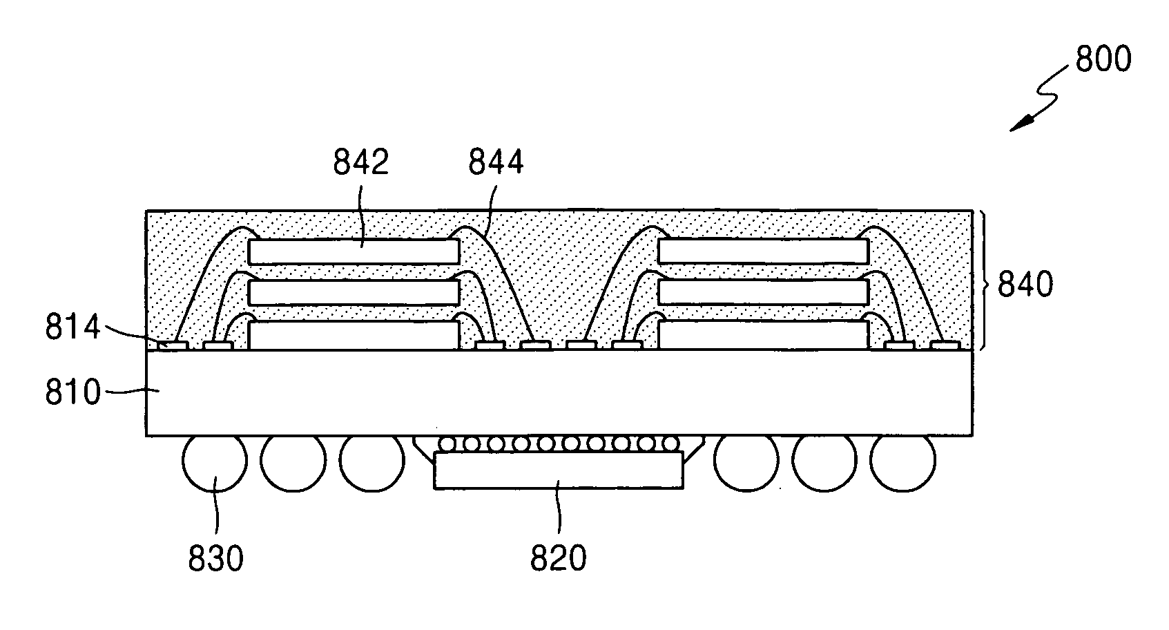
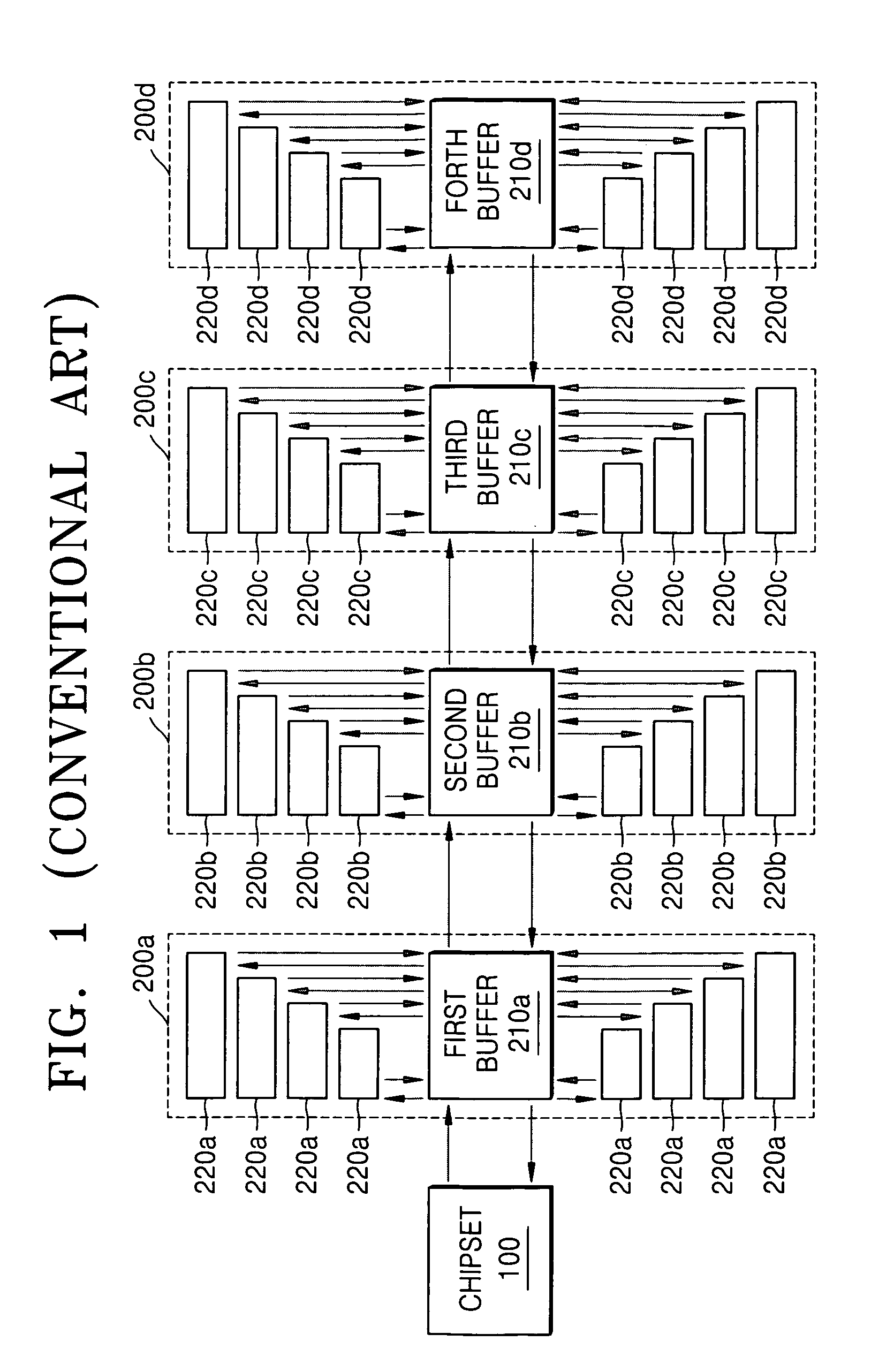
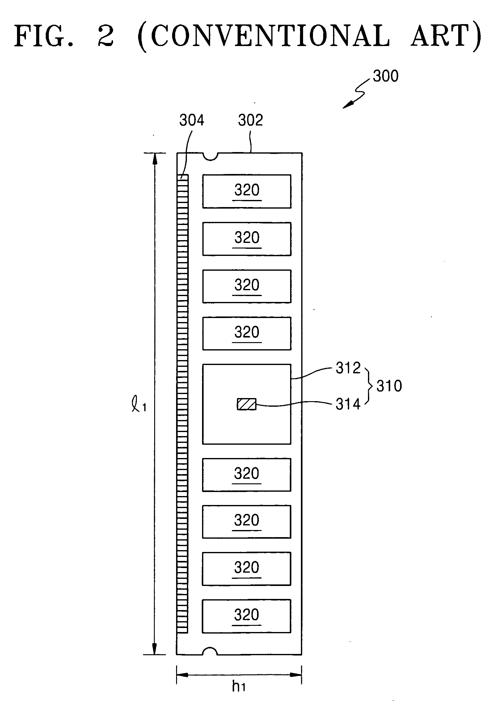
[0071] The present invention will now be described more fully with reference to the accompanying drawings in which exemplary embodiments of the invention are shown.

[0072] It should be noted that these Figures are intended to illustrate the general characteristics of methods and devices of exemplary embodiments of this invention, for the purpose of the description of such exemplary embodiments herein. These drawings are not, however, to scale and may not precisely reflect the characteristics of any given embodiment, and should not be interpreted as defining or limiting the range of values or properties of exemplary embodiments within the scope of this invention.

[0073] In particular, the relative thicknesses and positioning of layers or regions may be reduced or exaggerated for clarity. Further, a layer is considered as being formed “on” another layer or a substrate when formed either directly on the referenced layer or the substrate or formed on other layers or patterns overlaying ...


PUM


Abstract

A method and apparatus of fabricating a semiconductor device are disclosed. The semiconductor device may include a buffer chip package having a buffer chip mounted on a buffer chip substrate and at least one memory package mounted on the buffer chip substrate, wherein the at least one memory package may include a plurality of memory chips. Further, the buffer chip package may have a plurality of external connection terminals.

Description

BACKGROUND OF THE INVENTION [0001] This U.S. non-provisional application claims priority under 35 U.S.C. § 119 to Korean Patent Application No. 2004-24019, filed on Apr. 8, 2004, in the Korean Intellectual Property Office, the contents of which are incorporated by reference herein in their entirety. [0002] 1. Field of the Invention [0003] The present invention relates to a semiconductor device package, and more particularly, to a semiconductor device package with at least one buffered memory module. [0004] 2. Description of the Related Art [0005] A computer system may generally include a plurality of memory modules and at least one integrated circuit chipset (IC chipset) connected to the memory modules. The memory modules and the IC chipset may be connected using a memory interface which may transmit communication between them. As today's computer systems desire to improve performance, perform multi-tasking, and / or operate at higher speeds, the memory capacity may have to increase. ...

Claims


Application Information

Patent Timeline
Patent Type & Authority Applications(United States)
IPC IPC(8): G11C11/00H01L23/02H01L23/50H05K1/18
CPCH05K1/181H05K2201/10159H05K2201/10734H05K2203/1572H01L2924/15311H01L2924/19105H01L2224/48091H01L2924/00014H01L2224/16225H01L2224/32225H01L2224/48227H01L2224/73204Y02P70/611Y02P70/50H01L2924/00H01L23/50
Inventor LEE, JONG-JOOSONG, YOUNG-HEE
Owner SAMSUNG ELECTRONICS CO LTD
Why Eureka
Try Eureka