High performance stress-enhanced MOSFETs using Si:C and SiGe epitaxial source/drain and method of manufacture

a technology of stress-enhanced mosfets and epitaxial sources, which is applied in the direction of semiconductor devices, electrical equipment, transistors, etc., can solve the problems of significant increase in manufacturing time and cost, thick graded sige buffer layer cannot be easily applicable to silicon-on-insulator substrates (soi), and the structure of the sige buffer layer is too thick

Active Publication Date: 2005-04-21
AURIGA INNOVATIONS INC
View PDF99 Cites 223 Cited by
  • Summary
  • Abstract
  • Description
  • Claims
  • Application Information

AI Technical Summary

Benefits of technology

[0010] In a first aspect of the invention, a method of manufacturing a semiconductor structure includes forming a p-type field-effect-transistor (pFET) channel and a negative field-effect-transistor (nFET) channel in a substrate. A pFET stack and an nFET stack are formed on the substrate associated with the respective channels. A first layer of material is provided at source / drain regions associated with the pFET stack. The first layer of material has a lattice constant different than a base lattice constant of the substrate to create a compressive state within the pFET channel. A second layer of material is provided at the source / drain regions associated with the nFET stack. The second layer of material has a lattice constant different than the base lattice constant of the substrate to create a tensile state at the nFET channel.

Problems solved by technology

However, the same stress component, either tensile stress or compressive stress, discriminatively affects the characteristics of an n-type device and a p-type device.
However, the problem with this conventional approach is that it requires a multi-layered SiGe buffer layer that is very thick (e.g., a thickness of approximately 5000 Å to 15000 Å) to achieve misfit dislocations on its surface portion while avoiding threading dislocations between the SiGe layer and the silicon substrate layer, thereby achieving a relaxed SiGe structure on the surface of the multi-layered SiGe layer.
Also, this approach significantly increases manufacturing time and costs.
Further, the thick graded SiGe buffer layer cannot be easily applicable to silicon-on-insulator substrate (SOI).
The SiGe buffered layer structure is too thick.
Another problem is that misfit dislocations formed between the SiGe layer and the silicon epitaxial layer are random and highly non-uniform and cannot be easily controlled due to heterogeneous nucleation that cannot be easily controlled.
Also, misfit dislocation densities are significantly different from one place to another.
Thus, the physical stress derived from the non-uniform misfit dislocations are apt to be also highly non-uniform in the silicon epitaxial layer, and this non-uniform stress causes non-uniform benefits for performance with larger variability.
Further at those locations where misfit density is high, the defects degrade device performances through shorting device terminals and through other significant leakage mechanisms.
The problem with this approach is that the mobility is not enhanced, but retarded depending on the C content from scattering.

Method used


Image

  • High performance stress-enhanced MOSFETs using Si:C and SiGe epitaxial source/drain and method of manufacture
  • High performance stress-enhanced MOSFETs using Si:C and SiGe epitaxial source/drain and method of manufacture
  • High performance stress-enhanced MOSFETs using Si:C and SiGe epitaxial source/drain and method of manufacture

Examples


Embodiment Construction

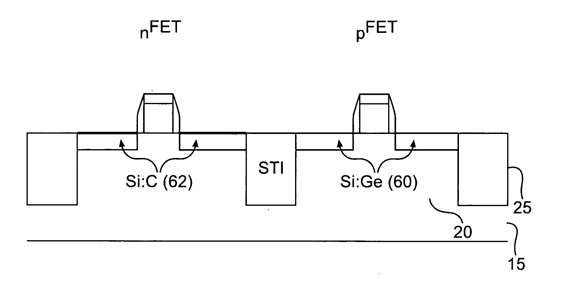
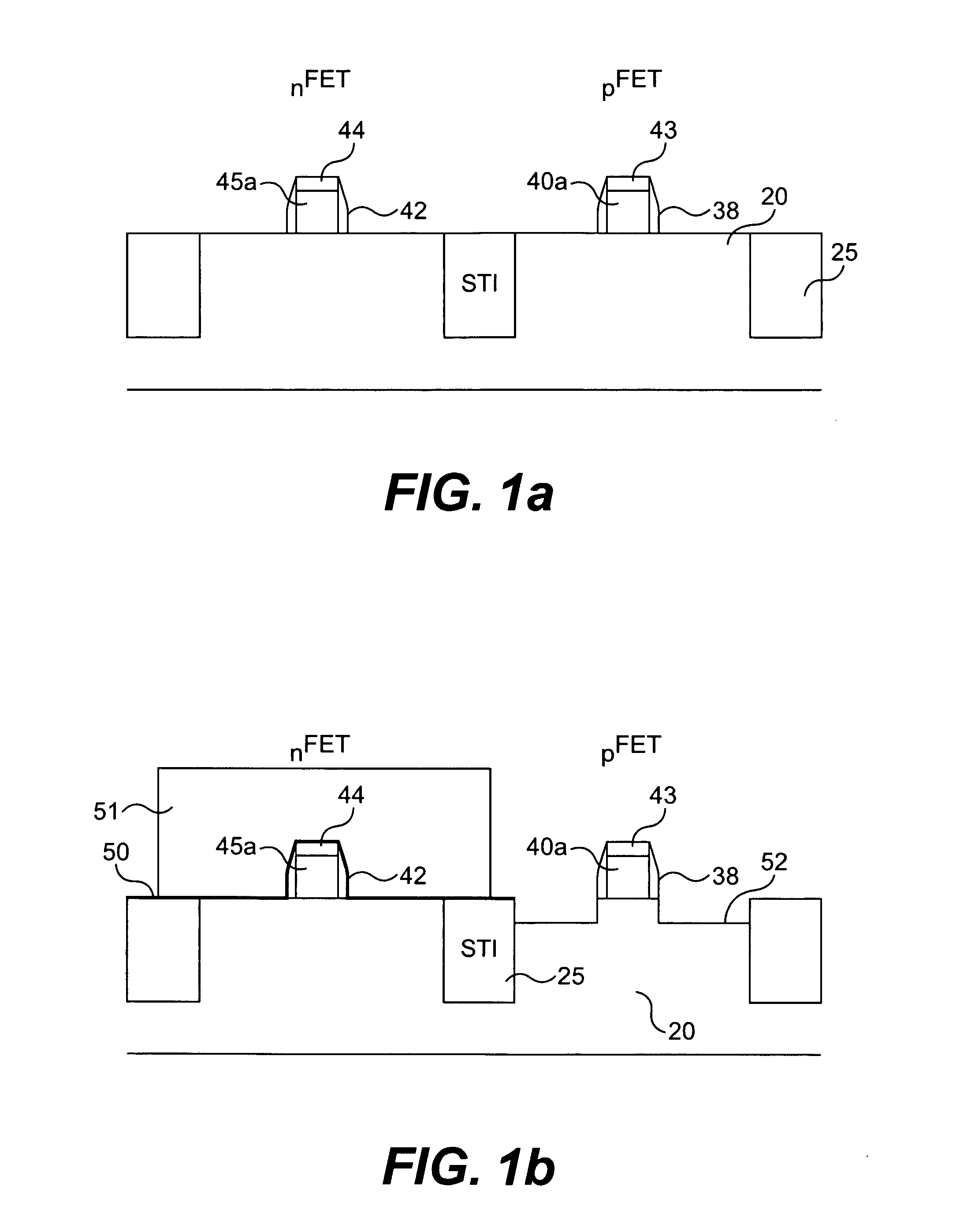
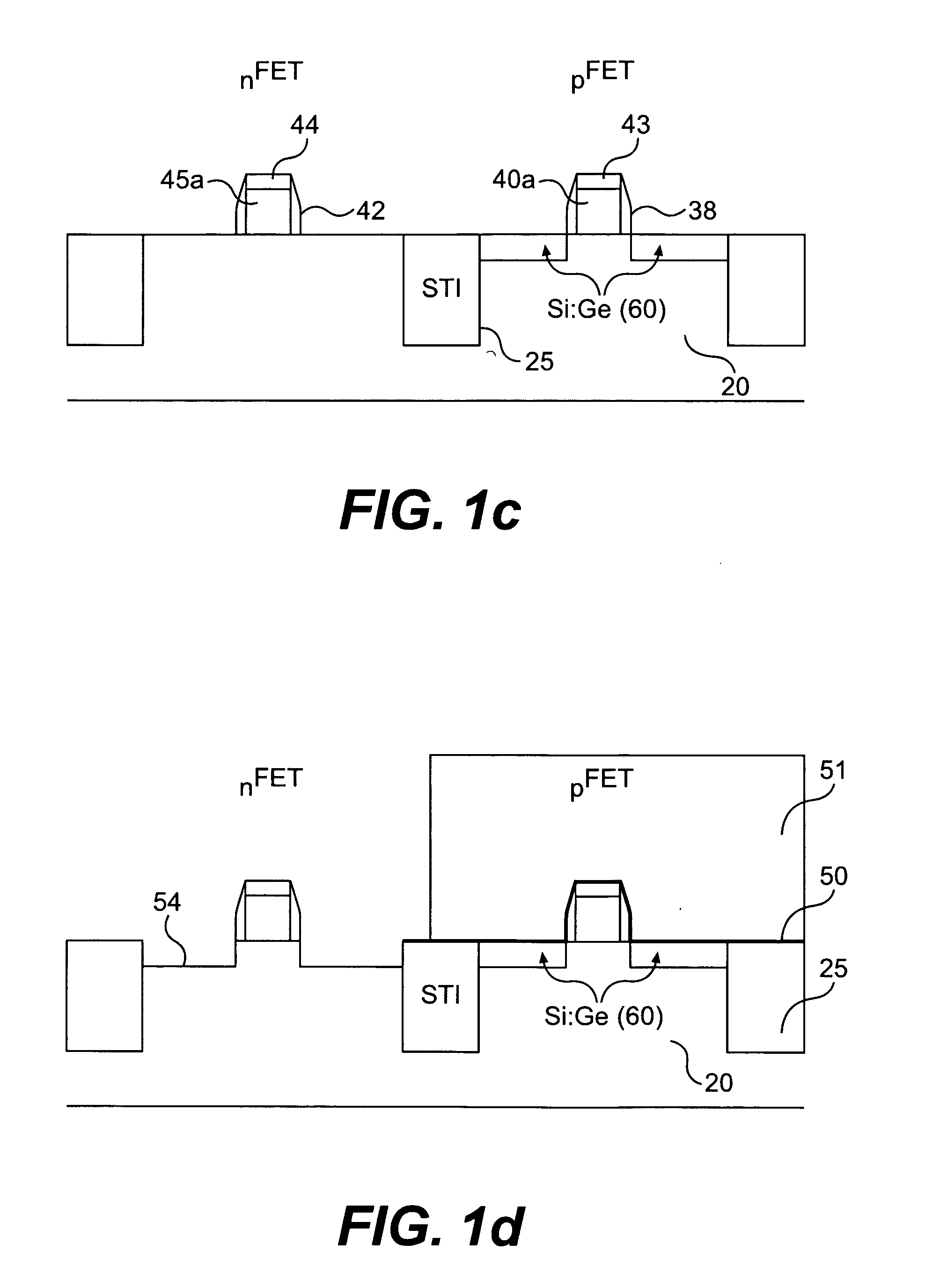
[0016] The invention is directed to a semiconductor device and method of manufacture which provides tensile stresses near the nFET channel and compressive stresses near the pFET channel of CMOS devices. In one embodiment of the invention, the longitudinal tensile stresses are brought very close to the nFET channel while at the same time compressive stresses are brought very close to the pFET channel. Additionally, in the invention, a process and structure is provided to integrate both SiGe and Si:C materials into CMOS technology.

[0017] By way of example, a highly tensile Si:C film is provided (e.g., embedded) in the silicon substrate in the source / drain (S / D) regions to longitudinally apply tension on the nFET structure in the channel under the gate region thereof. Similarly, a highly compressive SiGe film is provided (e.g., embedded) in the silicon substrate in the S / D regions to longitudinally apply compression on the pFET in the channel under the gate region thereof. Similar to ...


PUM


Abstract

A semiconductor device and method of manufacturing a semiconductor device. The semiconductor device includes channels for a pFET and an nFET. A SiGe layer is selectively grown in the source and drain regions of the pFET channel and a Si:C layer is selectively grown in source and drain regions of the nFET channel. The SiGe and Si:C layer match a lattice network of the underlying Si layer to create a stress component. In one implementation, this causes a compressive component in the pFET channel and a tensile component in the nFET channel.

Description

BACKGROUND OF THE INVENTION [0001] 1. Field of the Invention [0002] The invention generally relates to a semiconductor device and method of manufacture and, more particularly, to a semiconductor device and method of manufacture which imposes tensile and compressive stresses in the device during device fabrication. [0003] 2. Background Description [0004] Mechanical stresses within a semiconductor device substrate can modulate device performance. That is, stresses within a semiconductor device are known to enhance semiconductor device characteristics. Thus, to improve the characteristics of a semiconductor device, tensile and / or compressive stresses are created in the channel of the n-type devices (e.g., NFETs) and / or p-type devices (e.g., PFETs). However, the same stress component, either tensile stress or compressive stress, discriminatively affects the characteristics of an n-type device and a p-type device. [0005] For example, it has been known that a device exhibits better perfor...

Claims


Application Information

Patent Timeline
Patent Type & Authority Applications(United States)
IPC IPC(8): H01LH01L21/336H01L21/8238H01L21/84H01L27/01H01L27/12H01L29/10
CPCH01L21/823807H01L21/823814H01L29/1054H01L29/66628H01L29/66636H01L2924/0002H01L29/7848H01L27/092H01L2924/00H01L29/772H01L21/3081
Inventor CHEN, HUAJIECHIDAMBARRAO, DURESETIDOKUMACI, OMER H.
Owner AURIGA INNOVATIONS INC
Why Eureka
Try Eureka