
Microlens array imaging anticounterfeiting coin or badge
A micro-lens array and lens array technology, applied in the field of stamps and anti-counterfeiting coins, can solve the problems of limited application of coin anti-counterfeiting technology, and achieve the effect of good anti-counterfeiting effect and convenient identification.
Patent Information
- Authority / Receiving Office
- CN · China
- Patent Type
- Applications(China)
- Current Assignee / Owner
- Publication Date
- 2012-03-14
- Estimated Expiration
- Not applicable · inactive patent
Smart Images
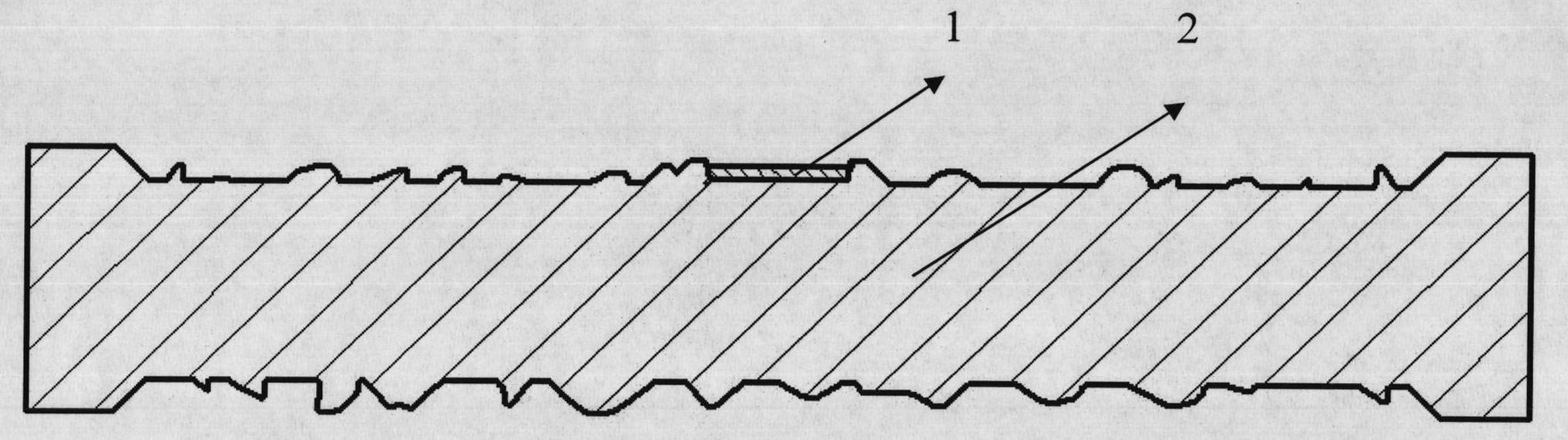
Figure 1 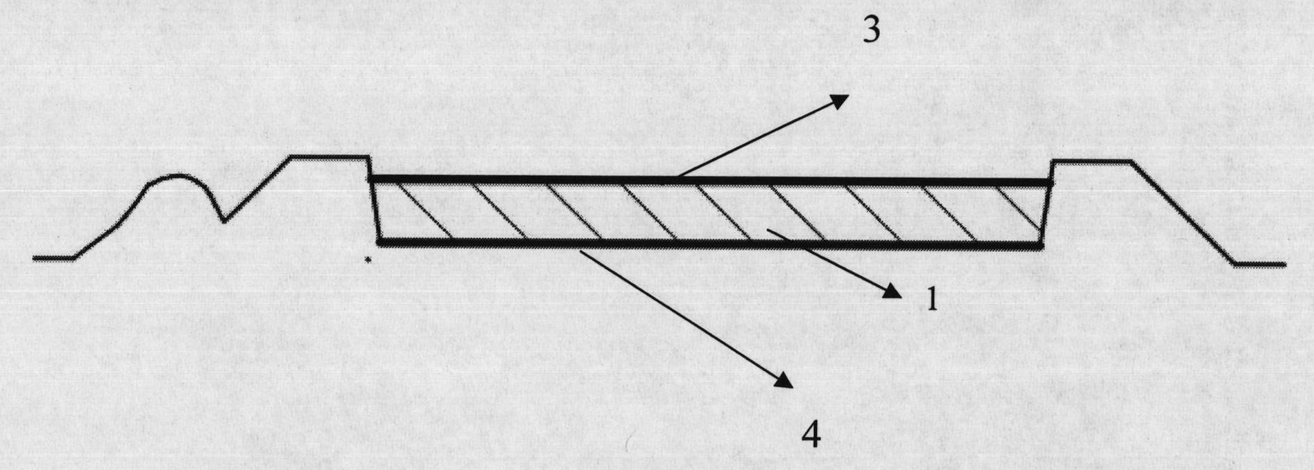
Figure 2 
Figure 3
Abstract
Description
technical field
[0001] The invention relates to an anti-counterfeit coin and stamp, in particular to a microlens array imaging anti-counterfeit coin and stamp. Background technique
[0002] At present, there are many kinds of anti-counterfeiting technologies applied to coins and chapters, including edge anti-counterfeiting, material, pattern anti-counterfeiting, etc. However, compared with other fields, the application of coin anti-counterfeiting technology is relatively limited. In recent years, many image anti-counterfeiting technologies have been successfully applied to coins, and have achieved good anti-counterfeiting effects, such as invisible engraving, laser holography, color pad printing and other technologies, which have greatly improved the anti-counterfeiting technical content of coins.
[0003] Coin designers are more willing to adopt anti-counterfeiting technology that intuitively expresses design ideas. The optical anti-counterfeiting technology that can be se...
Examples
Embodiment Construction
[0021] The present invention will be described in further detail below through the description of specific embodiment, but this is not limitation to the present invention, those skilled in the art can make various modifications or improvements according to the basic idea of the present invention, but as long as not departing from the principle of the present invention The basic ideas are all within the scope of the present invention.
[0022] Such as figure 1 As shown, it is a schematic cross-sectional structure diagram of micro-lens array imaging anti-counterfeiting coins and chapters. The present invention is composed of micro-pattern anti-counterfeiting patterns 4 and micro-lens signs, and micro-pattern anti-counterfeiting patterns 4 are directly printed on the surface of coins or chapters 2. A transparent medium 1 is coated on the pattern, and the transparent medium 1 is a thin layer of UV glue or other transparent medium to form a logo. The microlens array 3 structure i...