
Printed circuit board
A technology of printed circuit boards and conductive paths, applied in printed circuits, printed circuit components, circuits, etc., can solve the problems of electrical connectors that cannot meet the requirements and the characteristic impedance becomes smaller, and achieve the effect of improving the characteristic impedance and reducing the capacitance value
Patent Information
- Authority / Receiving Office
- CN · China
- Patent Type
- Applications(China)
- Current Assignee / Owner
- Publication Date
- 2012-05-23
- Estimated Expiration
- Not applicable · inactive patent
Smart Images
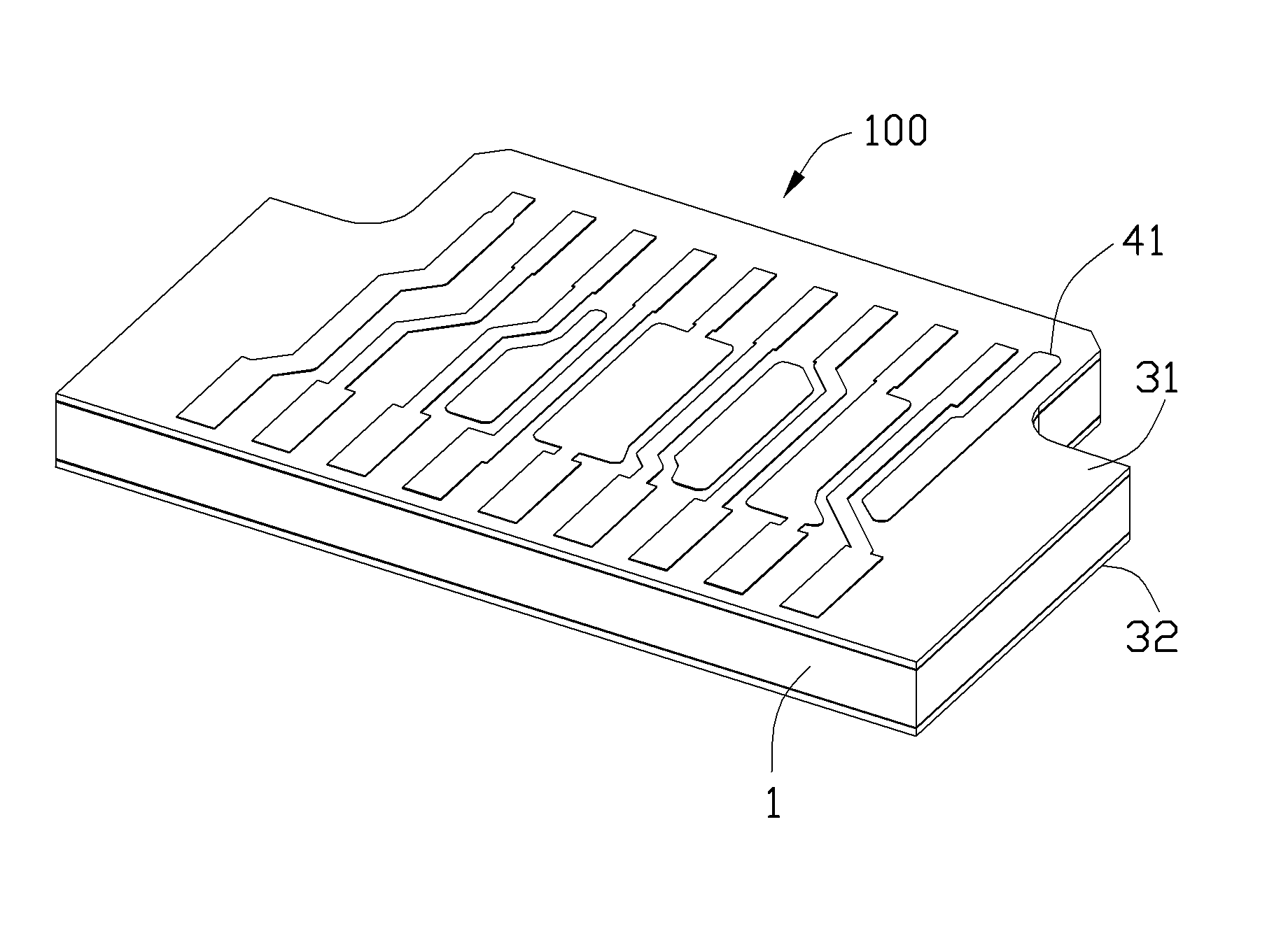
Figure 1 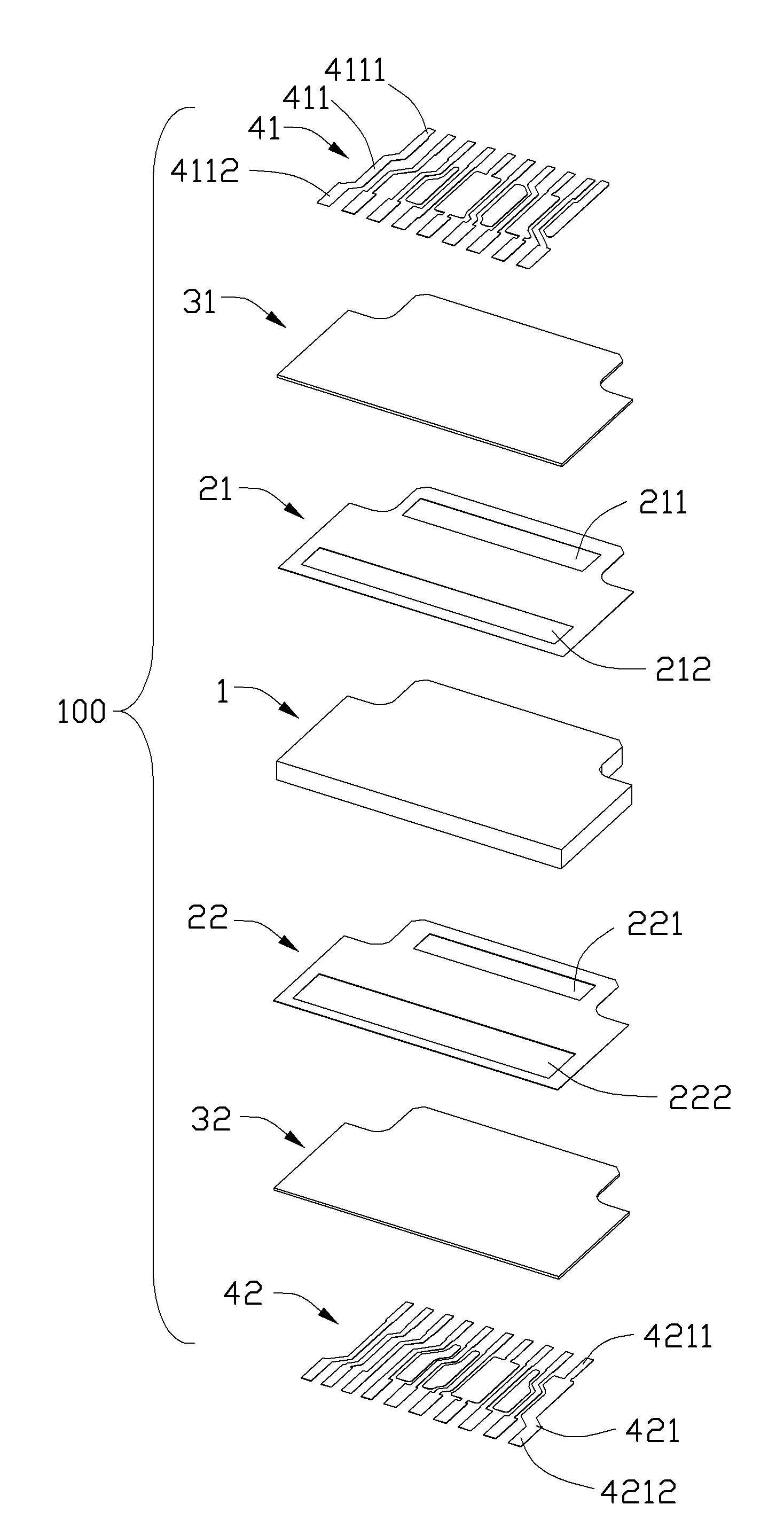
Figure 2 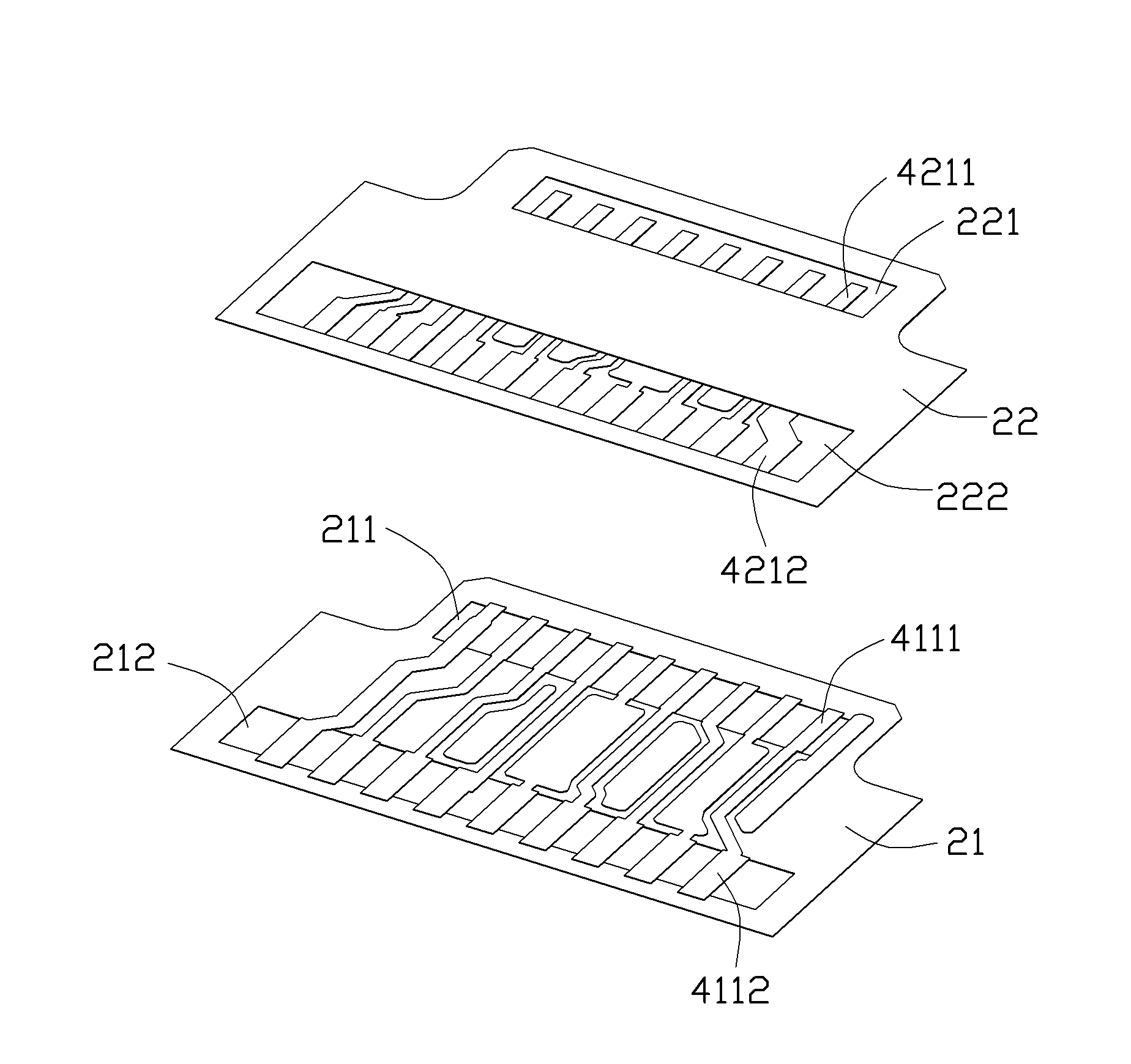
Figure 3
Abstract
Description
Technical Field
[0001] The invention relates to a printed circuit board, in particular to a printed circuit board inside an electrical connector for transmitting high frequency signals.
Background technique
[0002] With the rapid increase in signal transmission speed and the wide application of high-frequency circuits, higher requirements have been placed on printed circuit boards. The circuit performance provided by the printed circuit board must be able to ensure that the signal does not reflect during the transmission process, the signal remains intact, reduces the transmission loss, and plays the role of matching impedance, so as to obtain a complete, reliable, accurate, interference-free, and noise-free transmission signal. Printed circuit boards used in high-frequency electrical connectors are generally bonded together with several layers of materials. A traditional printed circuit board usually includes an insulating substrate, a ground layer, an interlayer, and a c...
Examples
Embodiment Construction
[0010] See Figure 1 to Figure 2 , The printed circuit board 100 of the present invention includes an insulating substrate 1, a first grounding layer 21, a second grounding layer 22, a first interlayer 31, a second interlayer 32, a first conductive path 41, and a second Conductive path 42. The printed circuit board 100 has a convex shape as a whole, but in other embodiments, it may also have other shapes.
[0011] The first ground layer 21 and the second ground layer 22 are printed by copper on the upper and lower surfaces of the insulating substrate 1, respectively. The first ground layer 21 is provided with a first through slot 211 at the front edge and a second through hole at the rear edge. The groove 212 and the second ground layer 22 are provided with a first through groove 221 at the front edge and a second through groove 222 at the rear edge. The first barrier layer 31 is located between the first ground layer 22 and the first conductive path 41, and the second barrier ...