
A resonant infrared detector structure and manufacturing method capable of isolating packaging stress
An infrared detector and packaging stress technology, applied in the direction of microstructure devices composed of deformable elements, microstructure technology, microstructure devices, etc., can solve the problems of increasing response time and so on
Patent Information
- Authority / Receiving Office
- CN · China
- Patent Type
- Patents(China)
- Current Assignee / Owner
- Publication Date
- 2019-04-16
- Estimated Expiration
- Not applicable · inactive patent
Smart Images
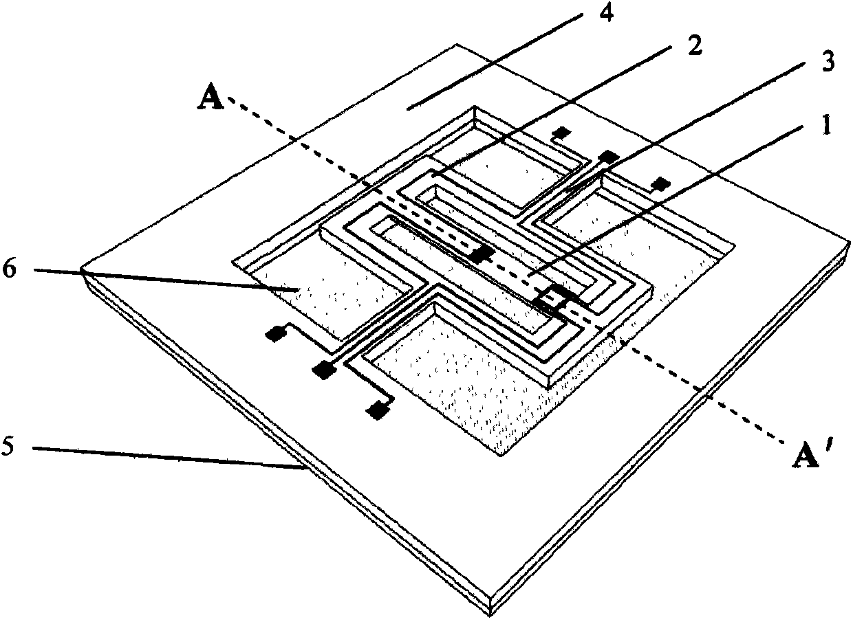
Figure 1 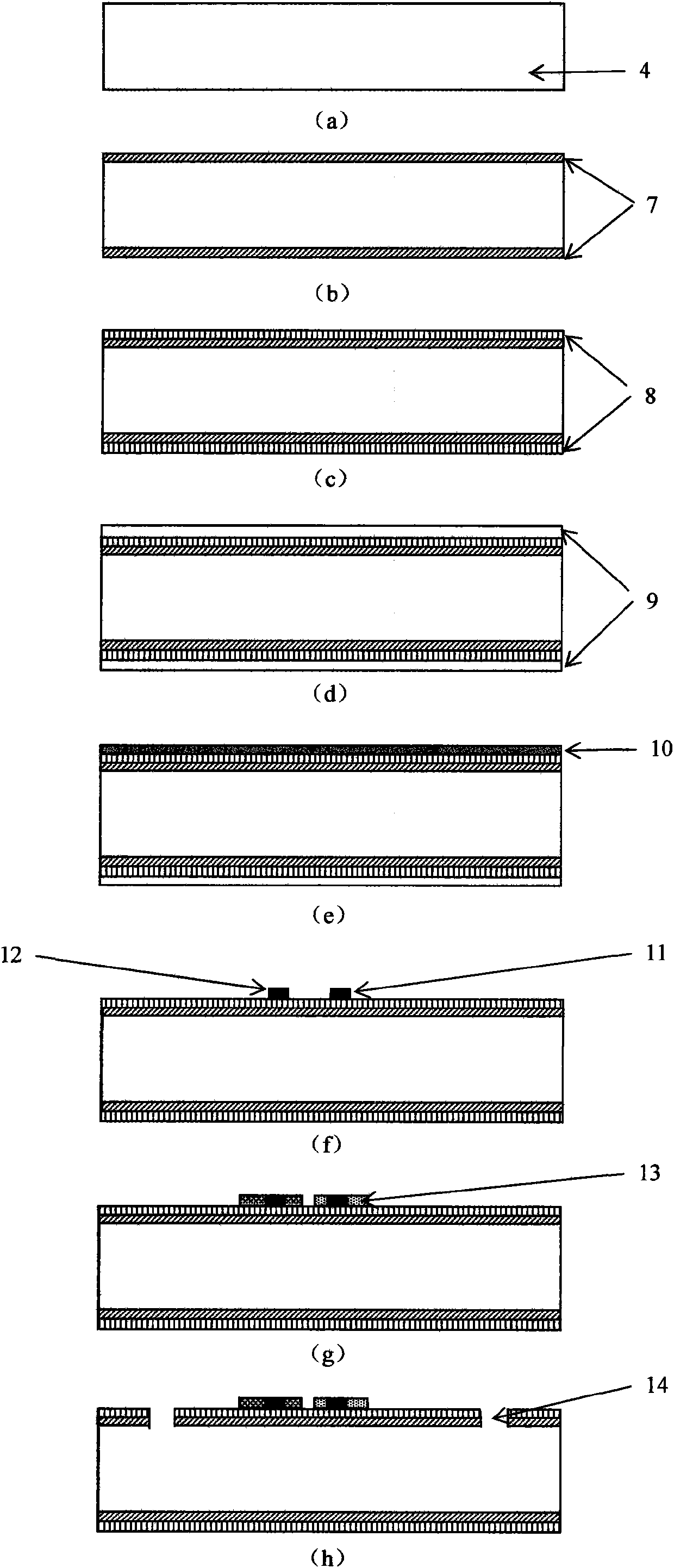
Figure 2 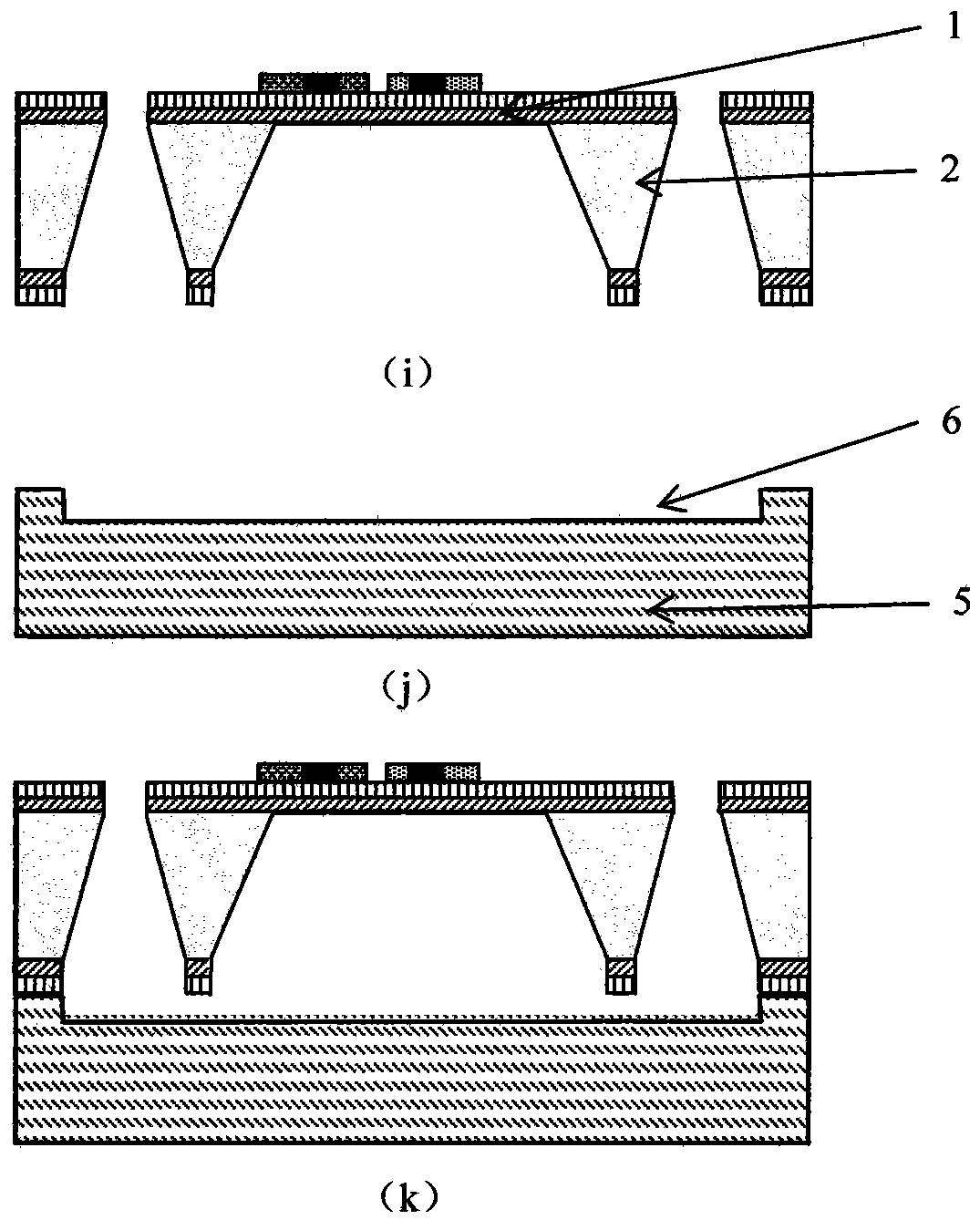
Figure 3
Abstract
Description
technical field
[0001] The invention relates to a structure and a manufacturing method of an infrared detector, in particular to a structure and a manufacturing method of a resonant infrared detector capable of isolating packaging stress, and belongs to the field of micro-electromechanical systems (MEMS). Background technique
[0002] According to the working principle, infrared detectors can be divided into two categories: cooled photon detectors and uncooled thermal detectors. The photon detector based on the photoelectric effect (photovoltaic effect, photoconductive effect, photoelectromagnetic effect and light emission effect) generated by the interaction between the incident photon flow and the detection material has good wavelength selectivity, short response time, and low noise equivalent temperature difference. It has a high detection rate and has been widely used in military fields such as aerospace, missile guidance, and infrared night vision. But photon detectors...
Examples
Embodiment 1
[0026] A resonant infrared detector capable of isolating packaging stress is manufactured by utilizing the technical scheme of the invention. Its micro-bridge resonator adopts polysilicon resistance electrothermal excitation and piezoresistive detection. Its production process is as follows:
[0027] (1) The original material is a double-sided polished silicon wafer of N-type, (100) plane, and resistivity 1-10Ω.cm. (see attached figure 2 (a))
[0028] (2) Thermally oxidize and grow a silicon dioxide film 7 with a thickness of 1 micron. (see attached figure 2 (b))
[0029] (3) A silicon nitride film 8 is deposited by a low-pressure chemical vapor deposition process (LPCVD), with a thickness of 0.3 microns. (see attached figure 2 (c))
[0030](4) Deposit a polysilicon film 9 with a thickness of 0.8 microns by a low-pressure chemical vapor deposition process (LPCVD). (see attached figure 2 (d))
[0031] (5) Ion implantation process Boron atoms are doped into the po...