
Exposure method
An exposure method and a technology to be exposed, which are applied in the field of exposure, can solve the problems of low etching rate, decreased etchant concentration, and large etching area, and achieve the effect of increasing pattern density and reducing lithography and etching deviations
Patent Information
- Authority / Receiving Office
- CN · China
- Current Assignee / Owner
- Publication Date
- 2014-12-17
Smart Images
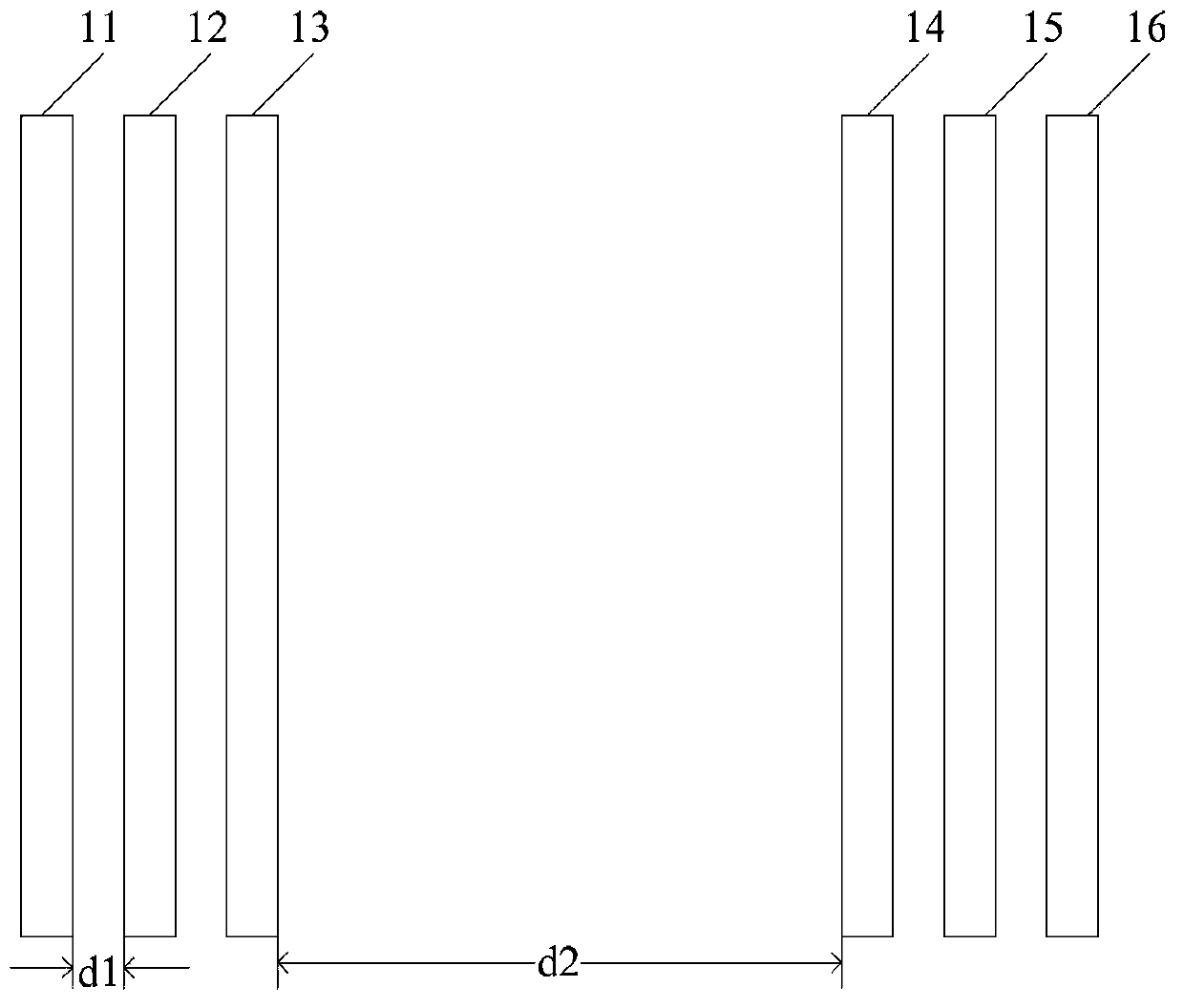
Figure 1 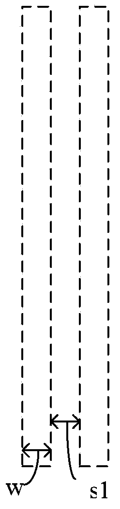
Figure 2 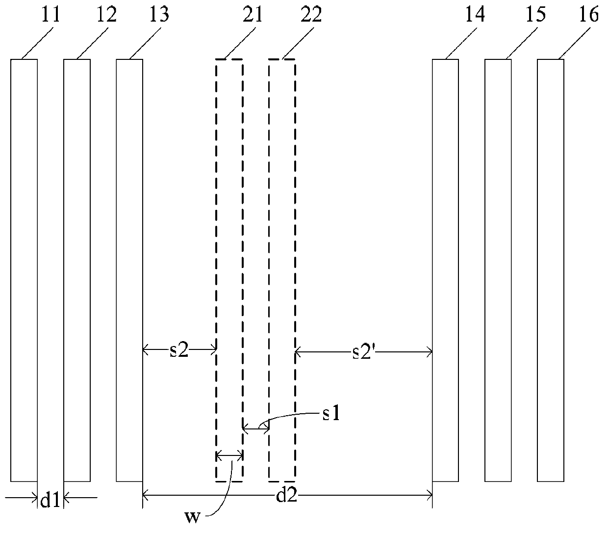
Figure 3
Abstract
Description
technical field
[0001] The present invention relates to the technical field of semiconductors, and in particular, to an exposure method. Background technique
[0002] As the critical dimensions of semiconductor devices are getting smaller and smaller, the use of a mask as a mask to form a patterning process under the traditional lithography process has encountered limitations, and the adjacent pattern spacing is too small, due to the optical proximity effect, there will be phase differences. The phenomenon of adjacent graphics sticking.
[0003] The above-mentioned problems can be solved by a double patterning method.
[0004] The double patterning method is to split the mask pattern to be formed into two sets of patterns, namely the first pattern and the second pattern, and then perform the first patterning on the mask layer to form the first pattern and the second pattern respectively. The sub-patterning forms a second pattern, and finally a complete mask pattern is form...
Examples
no. 1 example
[0034] Please refer to figure 1 , the to-be-exposed pattern has several patterns, and the to-be-exposed pattern has the patterns with two different pitches.
[0035] The to-be-exposed pattern may be any desired pattern in the actual layout design, the to-be-exposed pattern has several graphics, and the graphics need to be formed on the mask later. In the to-be-exposed pattern, there are at least two different spacings between the several patterns, and the size of the patterns meets the requirements of actual circuit design.
[0036] In this embodiment, the to-be-exposed pattern has several rectangular patterns with the same size and parallel to each other. The rectangular pattern is a pattern that appears frequently in chip design. In this embodiment, the patterns to be exposed include: a pattern 11 , a pattern 12 , a pattern 13 , a pattern 14 , a pattern 15 , and a pattern 16 . The to-be-exposed pattern has rectangular patterns with two different pitches, and the two diff...
no. 2 example
[0076] Please refer to Figure 10 , to provide a pattern to be exposed, the pattern to be exposed has several graphics, and the pattern to be exposed has the graphics with two different pitches.
[0077] The several patterns to be exposed include: a pattern 31 , a pattern 32 , a pattern 33 , a pattern 34 , a pattern to be exposed 35 , and a pattern 36 . The pattern has two different pitches d11 and d22.
[0078] In this embodiment, d11 is 32 nm, and the distance d22 between the pattern 33 and the pattern 34 to be exposed is 288 nm.
[0079] The same auxiliary patterns as in the first embodiment are provided, the width of the auxiliary patterns is 32 nm, and the spacing between adjacent auxiliary patterns is 32 nm. In this embodiment, the limit pitch of the single exposure is 64 nm. The critical dimension of the filling area is 224 nm, so the area between the to-be-pattern 33 and the pattern 34 is determined as the filling area, and more than two auxiliary patterns need to b...