
A Memory Compatible Method
A technology of memory and non-volatile flash memory, which is applied in the direction of assembling printed circuits with electrical components, and can solve problems that do not involve the technical characteristics of memory
Patent Information
- Authority / Receiving Office
- CN · China
- Patent Type
- Patents(China)
- Current Assignee / Owner
- Publication Date
- 2017-12-19
Smart Images
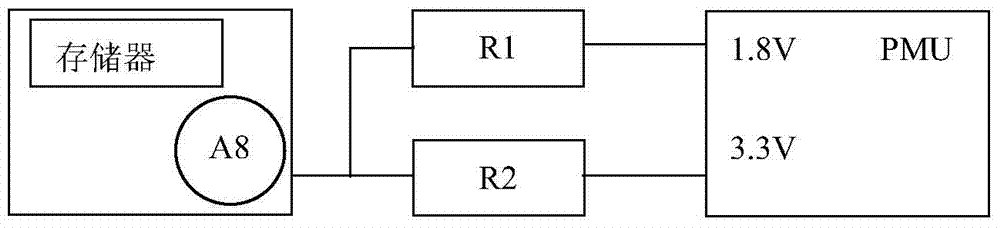
Figure 1 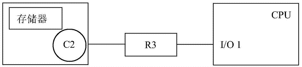
Figure 2 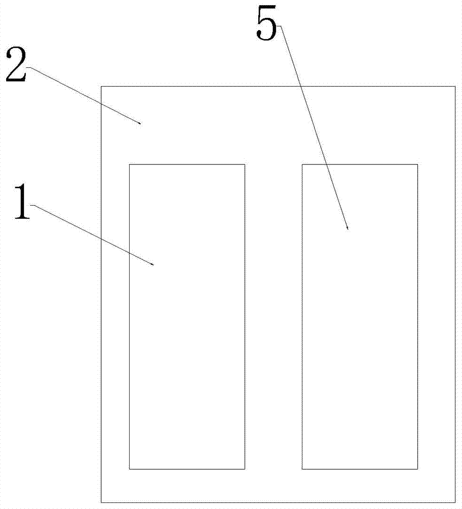
Figure 3
Abstract
Description
technical field
[0001] The invention relates to the field of semiconductor memory, in particular to a memory compatible method. Background technique
[0002] Among the current memory types, the packages of NAND (non-volatile flash memory) and EMMC (embedded flash memory) can be the same, but the working voltage and signal connection are different, and many CPUs (The central processing unit) can support two types of memory at the same time. If compatibility is achieved, an additional circuit needs to be added to control on-off. Such as figure 1 As shown, if the memory is NAND and its working voltage is 1.8V, then resistor R1 needs to be pasted, but resistor R2 is not; if the memory is EMMC and its working voltage is 3.3V, resistor R2 needs to be pasted instead of resistor R1 . Such as figure 2 As shown, I / O1 is a data input and output pin. If the memory is NAND, you need to paste resistor R3. If the memory is EMMC, you need to disconnect the signal of NAND, and do not pa...
Examples
Embodiment Construction
[0024] The present invention will be further described below in conjunction with the accompanying drawings and specific embodiments, but not as a limitation of the present invention.
[0025] In the field of semiconductors, the compatibility of memory NAND and EMMC can save costs, and has high versatility. All kinds of electronic products can be used, which is simple and convenient, and improves the market competitiveness of electronic products.
[0026] Therefore, the present invention designs a way to realize the compatibility of the above two memories. Originally, the two memories are connected to the CPU by adding an additional control circuit. Control the short connection and isolation between the pads by means of a method, which not only achieves the function of the original circuit, but also realizes the reduction of the functional area of the device and improves the performance of the product.
[0027] Such as image 3 , Figure 4 , Figure 5 As shown, the present...