
A kind of impurity removal method for semi-melted ingot of polycrystalline silicon
A polysilicon ingot furnace and polysilicon technology, applied in polycrystalline material growth, chemical instruments and methods, single crystal growth, etc., can solve problems such as large fluctuation range, ineffective removal of impurities and oxygen, and impact on product quality , to achieve the effect of low input cost, convenient realization and easy mastery
Patent Information
- Authority / Receiving Office
- CN · China
- Patent Type
- Patents(China)
- Current Assignee / Owner
- Publication Date
- 2018-10-12
- Estimated Expiration
- Not applicable · inactive patent
Smart Images
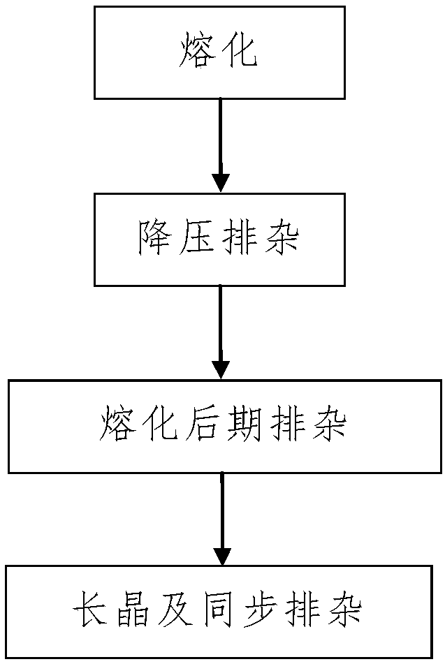
Figure 1 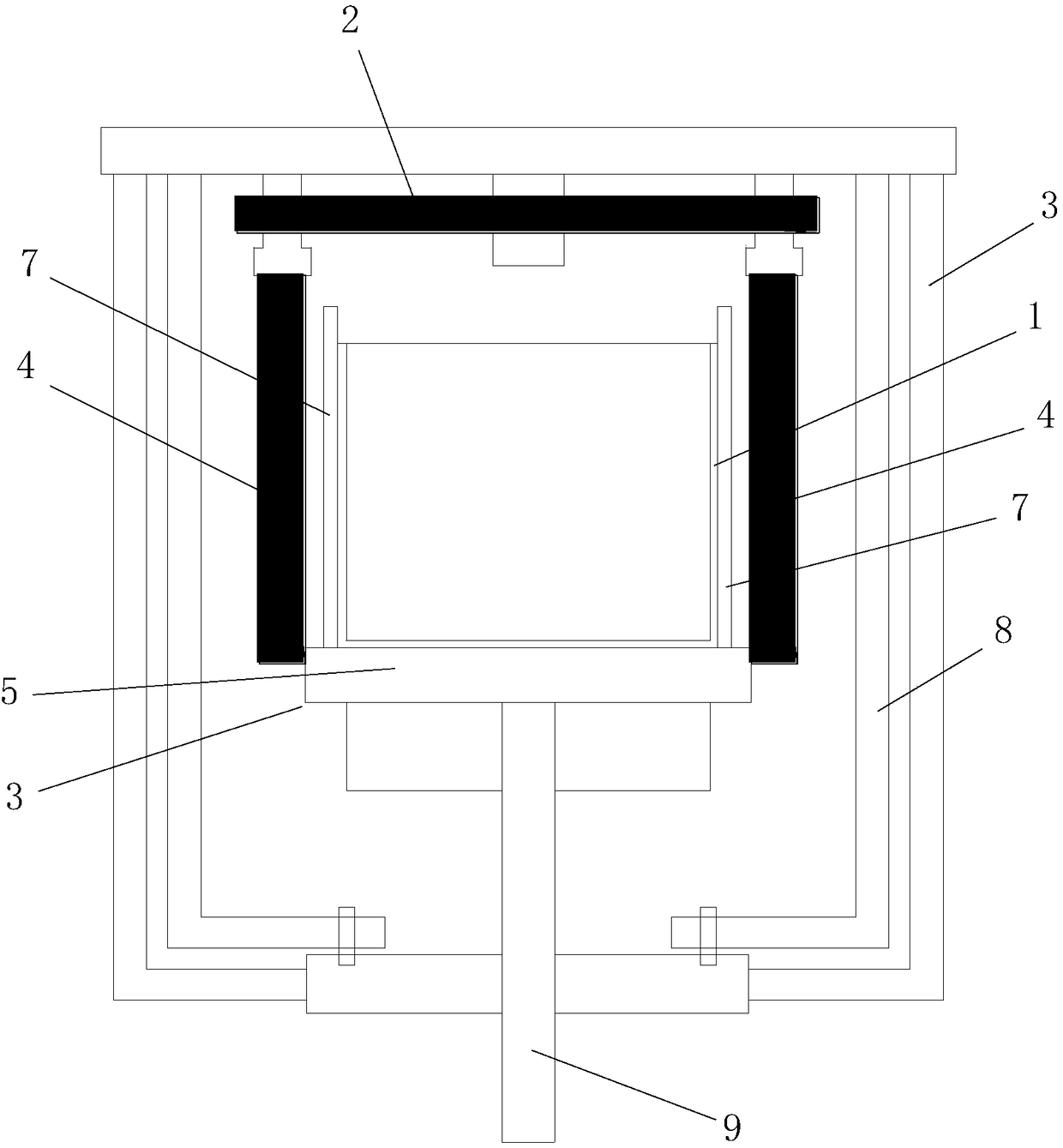
Figure 2 
Figure 3
Abstract
Description
technical field
[0001] The invention belongs to the technical field of polycrystalline silicon ingots, and in particular relates to a method for removing impurities for semi-melted polycrystalline silicon ingots. Background technique
[0002] Photovoltaic power generation is one of the most important clean energy sources with great development potential. The key factors restricting the development of photovoltaic industry are low photoelectric conversion efficiency on the one hand and high cost on the other hand. Photovoltaic silicon wafers are the basic material for the production of solar cells and components. The purity of polysilicon used to produce photovoltaic silicon wafers must be above 6N (that is, the total content of non-silicon impurities is below 1ppm), otherwise the performance of photovoltaic cells will be greatly negative influences. In recent years, the production technology of polycrystalline silicon wafers has made remarkable progress, and the polycrysta...
Examples
Embodiment 1
[0056] Such as figure 1 A kind of polysilicon semi-melting ingot shown is used for the impurity removal method, comprises the following steps:
[0057] Step 1, melting and removing impurities, the process is as follows:
[0058] Step 101, Melting: After turning on the top heater 2 located above the crucible 1 in the polysilicon ingot furnace 3 and the four side heaters 4 respectively arranged on the outside of the four side walls of the crucible 1, according to the conventional polysilicon semiconductor The ingot melting method uses a polycrystalline silicon ingot furnace 3 to melt the silicon material contained in the crucible 1, and the melting temperature is T1 to T2; wherein, T1=1200°C, T2=1540°C;
[0059] During the melting process in step 101, inert gas is filled into the polysilicon ingot furnace 3 and the air pressure in the polysilicon ingot furnace 3 is kept at Q1, wherein Q1=600mbar;
[0060] Step 102, step down and remove impurities, the process is as follows:
...
Embodiment 2
[0114] In this embodiment, the difference from Embodiment 1 is that the P described in step 1 dmax 150kW, P cmax =220kW; T1=1125 DEG C in step 101, T2=1530 DEG C, heat preservation 8h when carrying out the first heat preservation in step 1012, heat preservation 14h when carrying out the second heat preservation in step 1013; Q2=350mbar in the step 1021, step-down time It is 12min, and the holding time in step 1022 is 60min; The time for continuing to melt in step 103 is 40min, T3=1420°C; T4=1410°C in step 2, and c in step 201 1 =0.9, c 0 =0.6, the crystal growth time in the early stage is 15h; in step 202 T5=1405°C, the crystal growth time in the later stage is 35h; the crystal growth rate in step 2 is controlled at 10mm / h; Q1 in step 1 and step 2=550mbar.
[0115] In this embodiment, the remaining method steps and process parameters are the same as those in Embodiment 1.
[0116] In this embodiment, the surface of the processed polysilicon ingot has no impurities, no sticky ...
Embodiment 3
[0118] In this embodiment, the difference from Embodiment 1 is that the P described in step 1 dmax 180kW, P cmax =260kW; T1=1285 DEG C in step 101, T2=1550 DEG C, heat preservation 4h when carrying out the first time heat preservation in step 1012, heat preservation 10h when carrying out the second heat preservation in step 1013; Q2=450mbar in the step 1021, step-down time It is 8min, and the holding time in step 1022 is 10min; the time for continuing to melt in step 103 is 15min, T3=1440°C; T4=1430°C in step 2, c in step 201 1 =0.8,c 0 =0.3, the crystal growth time in the early stage is 10h; in step 202 T5=1425°C, the crystal growth time in the later stage is 28h; the crystal growth rate in step 2 is controlled at 13mm / h; Q1 in step 1 and step 2=650mbar.
[0119] In this embodiment, the remaining method steps and process parameters are the same as those in Embodiment 1.
[0120] In this embodiment, the surface of the processed polysilicon ingot has no impurities, no sticky...