
Plasma equipment for vapor phase etching and cleaning
A plasma and gas phase etching technology, used in electrical components, semiconductor/solid-state device manufacturing, discharge tubes, etc., can solve problems such as difficult processing, reduced productivity, increased maintenance costs, etc., to increase the amount of etching, increase the validity period, Choose a higher effect
Patent Information
- Authority / Receiving Office
- CN · China
- Patent Type
- Patents(China)
- Current Assignee / Owner
- Publication Date
- 2021-11-23
Smart Images
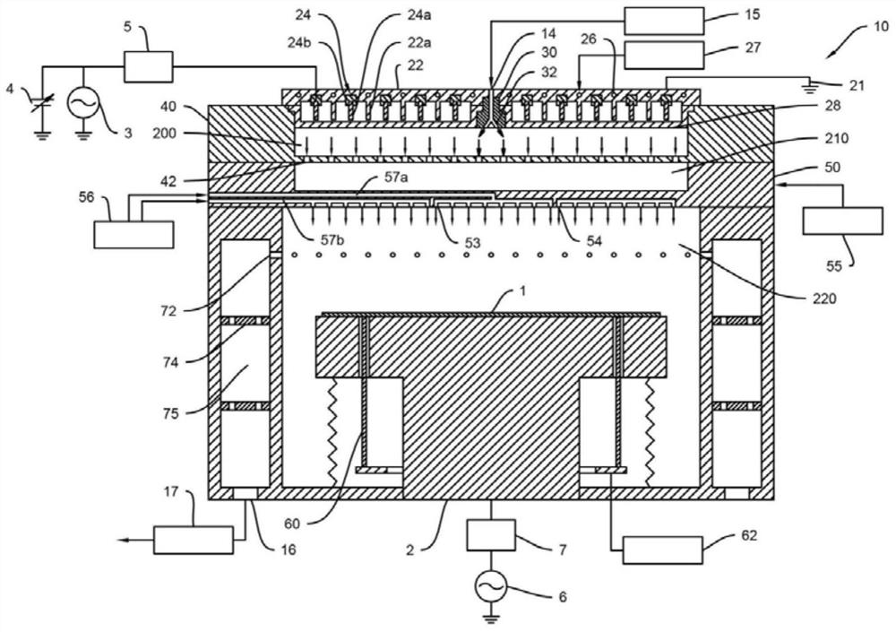
Figure 1 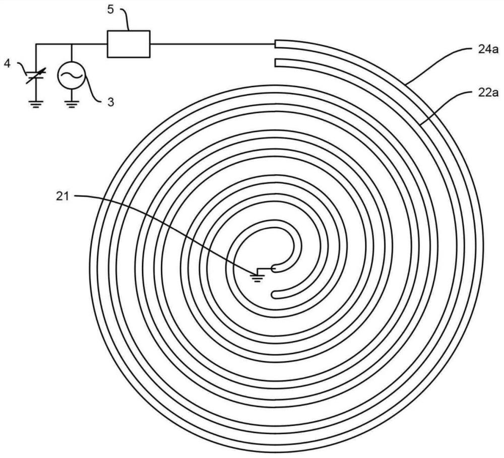
Figure 2 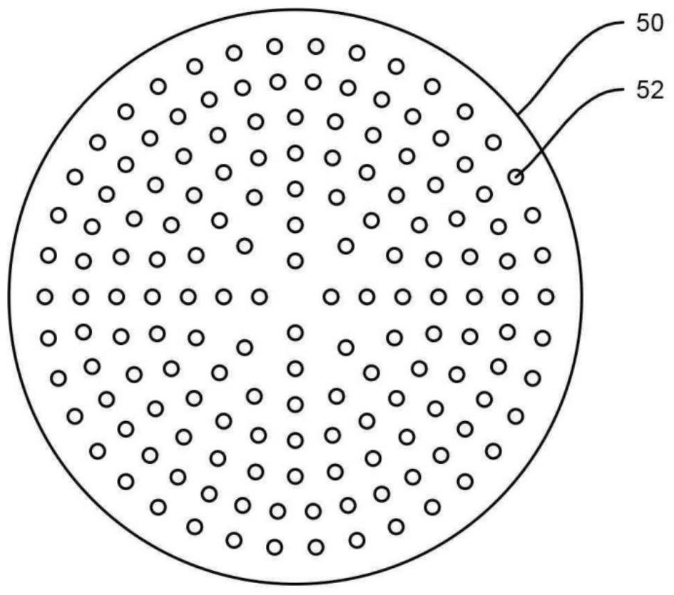
Figure 3
Abstract
Description
technical field
[0001] The present invention relates to a plasma device for gas-phase etching and cleaning, and in more detail, relates to a device for selectively cleaning by directly using highly reactive atoms or molecules to directly react with a thin film on the surface of a target substrate Plasma units for vapor phase etching and cleaning. Background technique
[0002] Semiconductors are active electronic components with functions such as storage, amplification, and switching of electronic signals, and have high integration, high performance, and low power consumption. They are high value-added and leading digital informatization in the traction system industry and service industry Core components of the era.
[0003] The semiconductor manufacturing process can be roughly divided into the front process (wafer processing process) and the back process (assembly process and inspection process), and the front process equipment accounts for about 75% of the market share. ...
Examples
Embodiment Construction
[0090] In order to fully understand the present invention, preferred embodiments of the present invention will be described below with reference to the accompanying drawings. The embodiments of the present invention can be changed in various forms, and the protection scope of the present invention is not limited to the embodiments described in detail below. This embodiment is provided to more fully describe the content of the present invention to those skilled in the art to which the present invention belongs. Therefore, in order to emphasize clearer description, the shapes of constituent members and the like in the drawings may be enlarged and shown. It should be noted that the same constituent members in the drawings are denoted by the same reference numerals. For well-known functions and constructions that are considered to obscure the gist of the present invention, detailed description thereof will be omitted.
[0091] figure 1 It is a figure showing the plasma processi...