
On-chip Hall Signal Amplifier and Method Based on Chopper Second-Order Compensation
A Hall signal, second-order compensation technology, applied in amplifiers, amplifiers with semiconductor devices/discharge tubes, improving amplifiers to reduce temperature/power supply voltage changes, etc. Good and other problems, to achieve the effect of cost increase and linearity improvement
Patent Information
- Authority / Receiving Office
- CN · China
- Patent Type
- Patents(China)
- Current Assignee / Owner
- Publication Date
- 2020-12-15
Smart Images
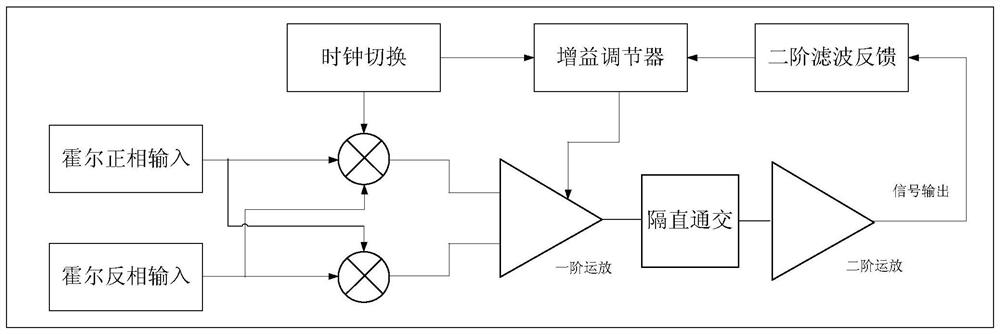
Figure 1 
Figure 2
Abstract
Description
technical field
[0001] The invention relates to the field of signal amplification, in particular to an on-chip Hall signal amplifier based on chopper second-order compensation and methods for eliminating offset and linear compensation. Background technique
[0002] In the design of integrated circuits, there are often problems such as operational amplifier misalignment, excessive voltage, excessive temperature drift of devices, and poor linearity characteristics during small signal amplification.
[0003] In order to solve the above problems, technicians often need to do zero drift, temperature drift elimination, and linearity compensation for the signal conditioning amplifier circuit. The problem is that the characteristics of the tubes at the forward and reverse ends of the operational amplifier are inconsistent, and the voltage is out of balance during static operation. If the silicon-based Hall signal is directly amplified, the weak signal is easily overwhelmed by the of...
Examples
Embodiment Construction
[0032] The present invention will be further described in detail below in conjunction with the accompanying drawings and embodiments.
[0033] Such as figure 1 Shown is an on-chip Hall signal amplifier based on chopper second-order compensation, including:
[0034] The signal input module provides the Hall positive-phase input signal and negative-phase input signal to the chopper modulation module;
[0035] The chopping modulation module is connected to the two output terminals of the signal input module, and modulates and outputs the positive-phase input signal and the negative-phase input signal; the chopping modulation module is composed of two mixers;
[0036] The clock module provides switching frequency and modulation frequency for the chopping modulation module; the chopping modulation module switches the input signal between positive phase and negative phase based on the switching frequency of the clock module, and modulates the offset voltage in the input signal to ...