
Terahertz antenna structure and radiation source and detector comprising same
An antenna structure and terahertz technology, applied in the terahertz field, can solve the problems of low matching efficiency between terahertz antennas and photoconductors, reduce antenna input resistance, etc., and achieve the effects of improving detection sensitivity, increasing input resistance, and small absorption coefficient
Patent Information
- Authority / Receiving Office
- CN · China
- Patent Type
- Applications(China)
- Current Assignee / Owner
- Publication Date
- 2018-09-04
Smart Images
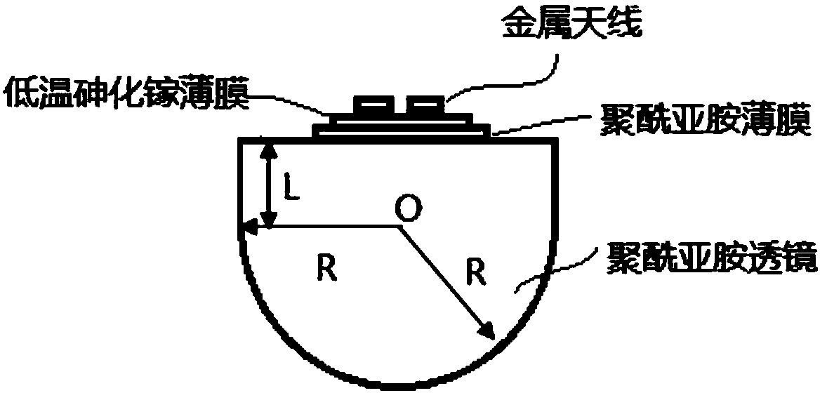
Figure 1 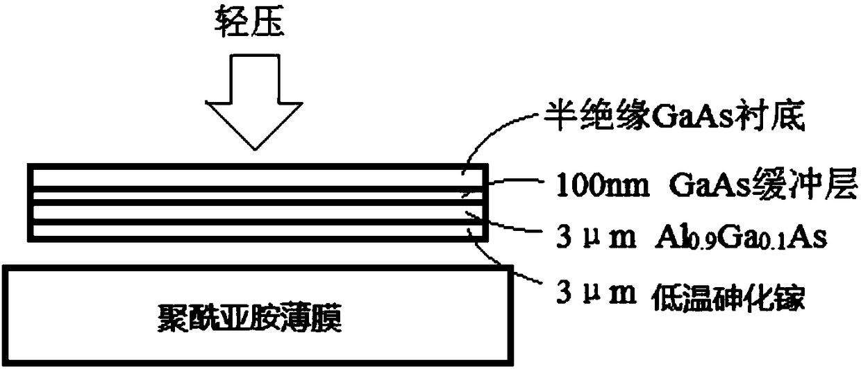
Figure 2 
Figure 3
Abstract
Description
technical field
[0001] The invention belongs to the technical field of terahertz, and in particular relates to a terahertz antenna structure and a radiation source and a detector including the antenna structure. Background technique
[0002] Terahertz radiation is an electromagnetic wave with a frequency between 0.1THz and 10THz, which has great application prospects in security inspection, medical treatment, communication and other fields. For a long time, the development of terahertz sources (radiation sources) with high radiation intensity has been one of the key technologies of terahertz technology. Among them, the photoconductive antenna technology based on semiconductor materials has the advantages of working at room temperature, portability, and low price. However, due to the high resistivity of semiconductor materials, the resistance of the photoconductor in the illuminated gap area of the antenna is generally above 10,000 ohms, while the input resistance of the p...
Examples
Embodiment 1
[0029] The traditional terahertz antenna processing method is to evaporate a metal antenna on a semiconductor substrate with a thickness of 300 microns, and then directly paste a silicon lens on the back. Because the semiconductor substrate of the structure of the present invention is only several microns thick, the traditional substrate thinning process is no longer applicable, and needs to be prepared by the following method: first, by epitaxial layer transfer technology, the semiconductor substrate film is transferred from The sacrificial layer is peeled off and transferred to a substrate of low dielectric constant material. Then the metal antenna is evaporated on the semiconductor substrate film. Finally, a lens made of low dielectric constant material is pasted on the back. The specific structure is as figure 1 with figure 2 shown. Specifically as follows:
[0030] A 100nm-thick GaAs buffer layer was grown on a (100)-oriented semi-insulating GaAs substrate by molecu...