
Electric injection annealing device
An annealing device, a technology of current injection, applied in circuits, electrical components, sustainable manufacturing/processing, etc., to achieve the effect of improving conversion efficiency, high processing efficiency, and high-efficiency annealing effect
Patent Information
- Authority / Receiving Office
- CN · China
- Patent Type
- Applications(China)
- Current Assignee / Owner
- Publication Date
- 2018-09-07
Smart Images
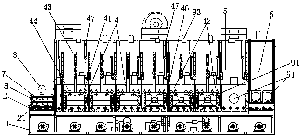
Figure 1 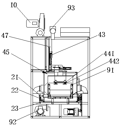
Figure 2 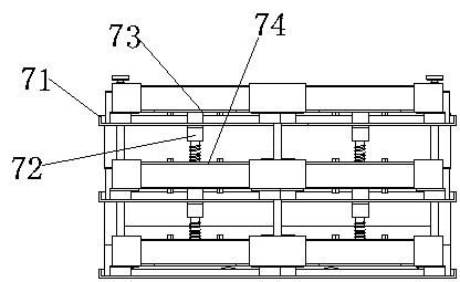
Figure 3
Abstract
Description
technical field
[0001] The invention relates to the technical field of cell sheet processing, in particular to a device for annealing a cell sheet, in particular to an electric injection annealing device. Background technique
[0002] The silicon wafer (battery) contains oxygen, which has the function of absorbing impurities. Annealing the silicon wafer can promote the outward diffusion of oxygen remaining in the silicon, forming a low-oxygen environment (clean area) on the surface of the silicon wafer, thereby Reducing or even eliminating crystal defects caused by oxygen is beneficial to later device manufacturing, and annealing of silicon wafers can affect its resistivity and minority carrier lifetime. In addition, light-induced degradation (LID) refers to the power attenuation phenomenon caused by solar cells and components during the illumination process. In order to improve battery efficiency, PERC (passivated emitter and back local contact cell) high-efficiency batter...
Examples
Embodiment Construction
[0036] The technical solutions of the present invention will be clearly and completely described below in conjunction with the accompanying drawings. Apparently, the described embodiments are some of the embodiments of the present invention, but not all of them. Based on the embodiments of the present invention, all other embodiments obtained by persons of ordinary skill in the art without making creative efforts belong to the protection scope of the present invention.
[0037] In the description of the present invention, it should be noted that the terms "center", "upper", "lower", "left", "right", "vertical", "horizontal", "inner", "outer" etc. The indicated orientation or positional relationship is based on the orientation or positional relationship shown in the drawings, and is only for the convenience of describing the present invention and simplifying the description, rather than indicating or implying that the referred device or element must have a specific orientation, ...