
Electrically injected silicon-based III-V group edge-emitting nanowire laser and its preparation method
A III-V and nanowire technology, applied in the field of optoelectronics, can solve problems such as easy leakage of photons, absence of optical modes, breakage of III-V nanowires, etc., to achieve the effect of facilitating coupling and preventing leakage
Patent Information
- Authority / Receiving Office
- CN · China
- Patent Type
- Patents(China)
- Current Assignee / Owner
- Publication Date
- 2020-05-19
Smart Images
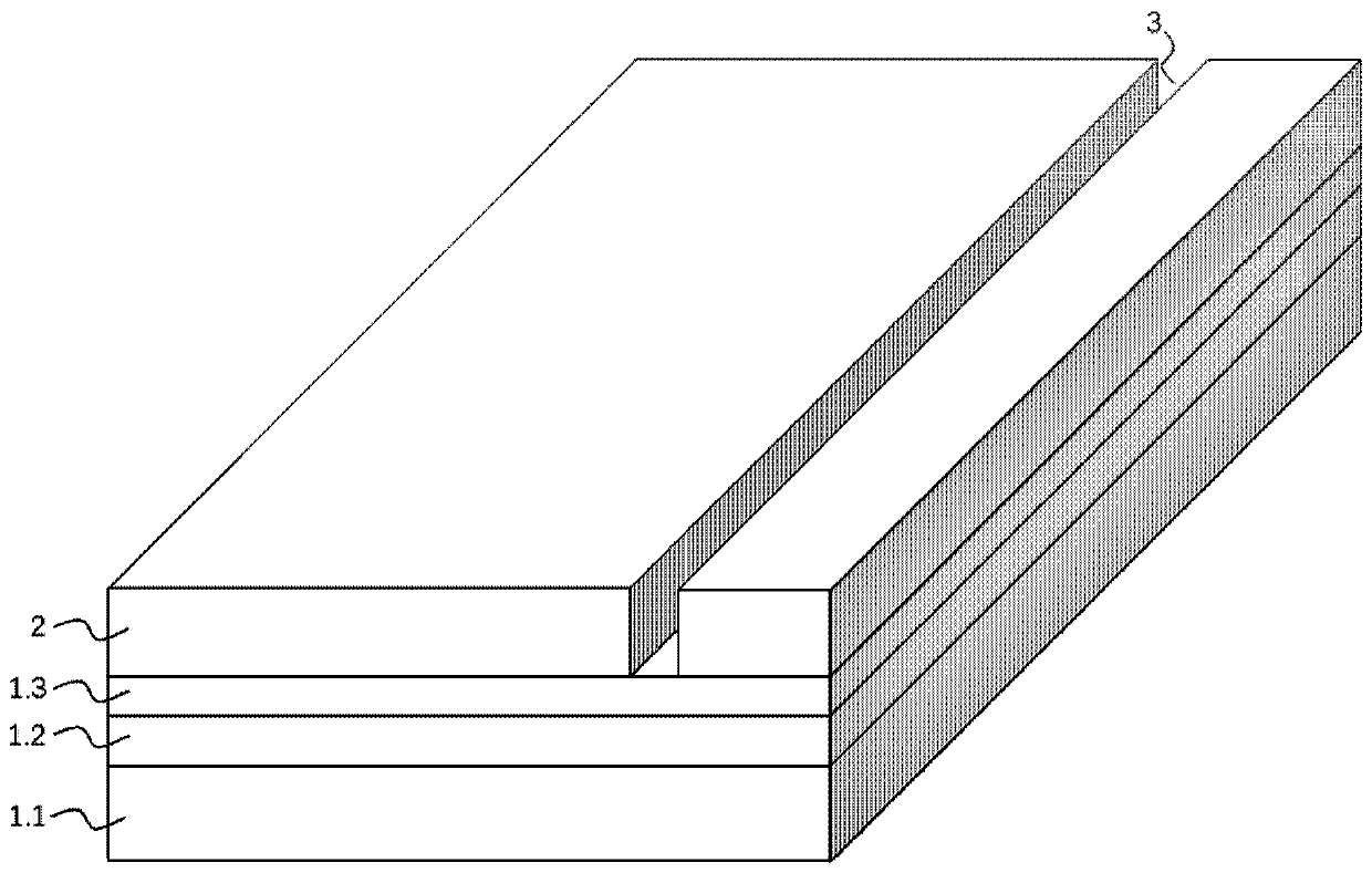
Figure 1 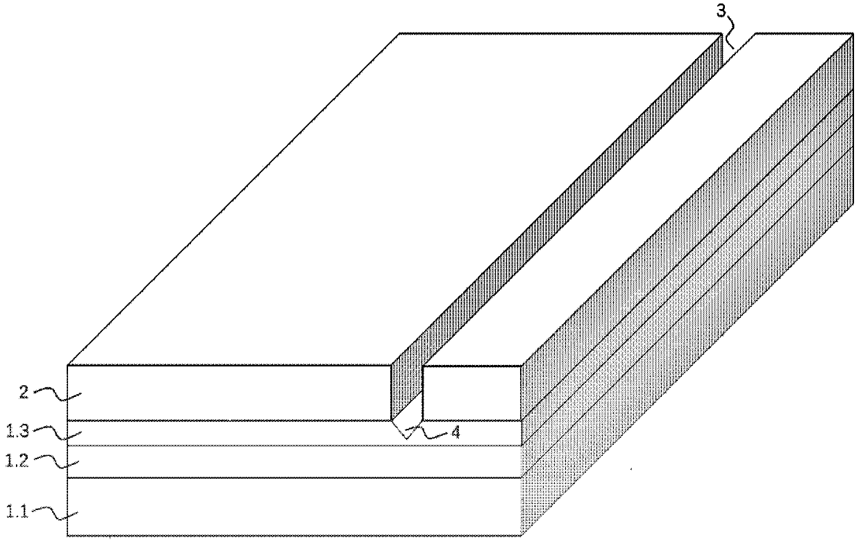
Figure 2 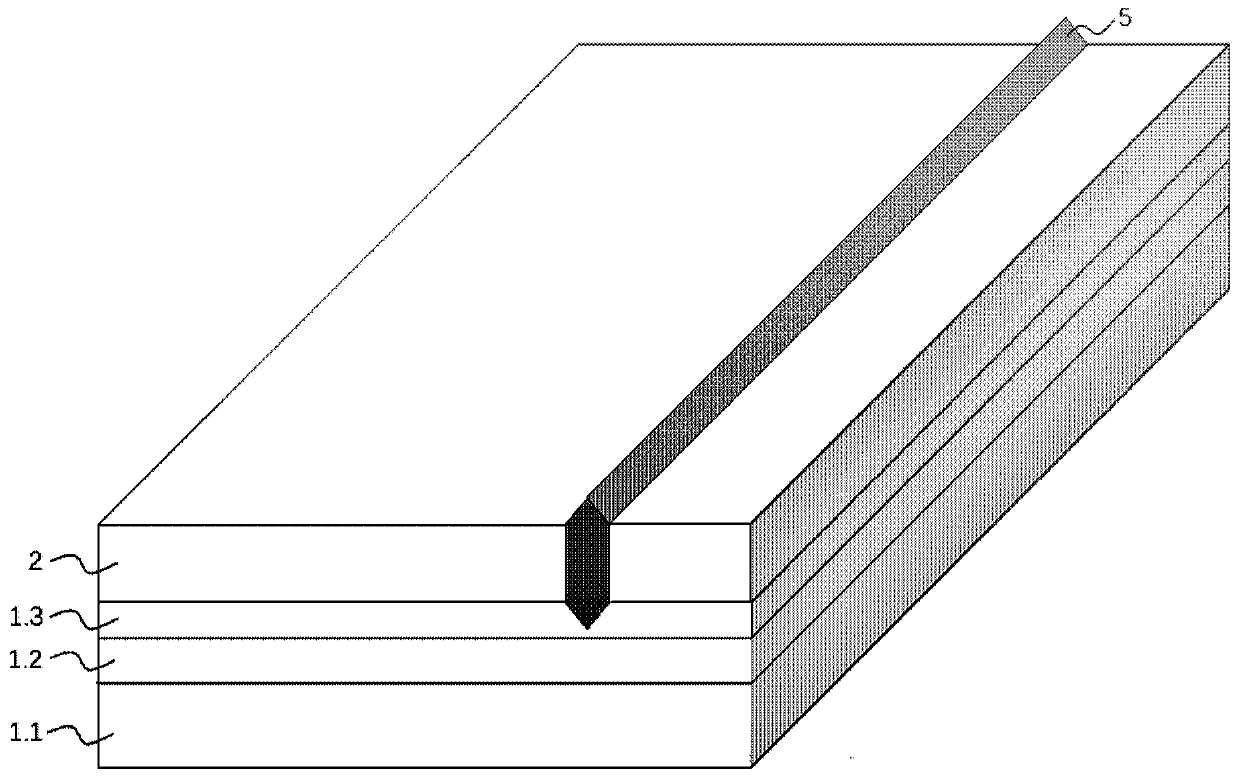
Figure 3
Abstract
Description
Technical field
[0001] The invention relates to the technical field of optoelectronics, in particular to an electrically injected silicon-based III-V group edge-emitting nanowire laser and a preparation method thereof. Background technique
[0002] Since the birth of the first integrated circuit, integrated circuit technology has maintained an ultra-high-speed development, and MOSFET devices with silicon as a substrate have become the core and foundation of modern integrated circuit technology. As the feature size of devices continues to shrink, integrated circuit technology is limited by a series of basic physical issues and process technology in terms of speed, power consumption, integration, and reliability. In order to achieve greater storage capacity and higher transmission speed, the traditional communication technology that uses electrons as information transmission carriers can no longer meet the needs of practical applications, and it has become a mainstream development ...
Examples
preparation example Construction
[0055] According to an embodiment of the present invention, there is provided a method for preparing an electrically implanted silicon-based III-V group edge-emitting nanowire laser, including:
[0056] Depositing a silicon dioxide layer on the SOI substrate, and etching rectangular trenches on the silicon dioxide layer;
[0057] Etching a v-shaped groove in the top silicon of the SOI substrate under the rectangular groove to communicate with the rectangular groove to form a connecting groove;
[0058] Growing a silicon-based III-V family side-emitting nanowire laser epitaxial structure in the connecting trench;
[0059] A metal electrode is prepared on the silicon-based III-V group side-emitting nanowire laser.
[0060] The invention provides a process method for realizing electrical injection for III-V family nanowire materials epitaxially on an SOI substrate, and the prepared electrode can be used to test the dynamic characteristics of silicon-based III-V family side-emitting nanowir...