
Simulation test method for instantaneous dose rate effect of module-level circuit
A dose rate effect and simulation test technology, applied in dosimeters, electrical digital data processing, special data processing applications, etc., can solve the problem of insufficient research and prediction ability of instantaneous dose rate effect, and achieve the effect of improving the prediction ability.
Patent Information
- Authority / Receiving Office
- CN · China
- Patent Type
- Applications(China)
- Current Assignee / Owner
- Publication Date
- 2020-12-04
Smart Images
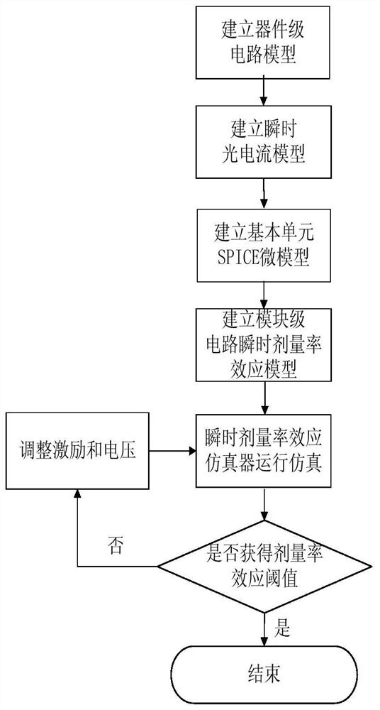
Figure 1
Abstract
Description
technical field
[0001] The invention relates to a simulation test method for instantaneous dose rate effect of a module-level circuit, belonging to the technical field of simulation test of integrated circuit radiation effect. Background technique
[0002] As the semiconductor process enters the nanotechnology process, the sensitive volume of the device continues to shrink, the operating voltage and device capacitance decrease, resulting in a continuous decrease in the critical charge, while the parasitic effect continues to increase, resulting in a circuit response to the instantaneous dose rate effect that is different from that of a large size. different characteristics of the device circuit. The performance index of integrated circuits is getting higher and higher, the scale is getting bigger and bigger, and the circuit structure is becoming more and more complex. There are many factors that affect the radiation effect of dose rate and affect each other. Instantaneous do...
Examples
Embodiment
[0064] This embodiment provides a simulation method for the instantaneous dose rate effect of a trigger module circuit, including the following steps:
[0065] Step 1: Select a typical flip-flop module level circuit, carry out the device physical model establishment of the basic unit PMOS tube and NMOS tube according to the method given in the present invention, obtain the current waveform and voltage change with time and the corresponding internal current carrying The electrical parameters are obtained through the change of sub-units; and the process alignment is carried out with the electrical characteristic curves of the basic unit NMOS transistor and PMOS transistor of the device-level circuit in SPICE, and a relatively accurate physical model of the device-level circuit is obtained.
[0066] Step 2: According to the product structure and process of the flip-flop circuit, determine the junction depth, electron-hole pair mobility, majority carrier concentration, hole lifetim...