
Array substrate and preparation method thereof
An array substrate and substrate technology, applied in the field of array substrate and its preparation, can solve the problems of high production cost, long cycle, cumbersome preparation method steps, etc., and achieve the effects of improving production capacity, reducing production cost and reducing production process
Patent Information
- Authority / Receiving Office
- CN · China
- Patent Type
- Applications(China)
- Current Assignee / Owner
- Publication Date
- 2021-03-23
- Estimated Expiration
- Not applicable · inactive patent
Smart Images
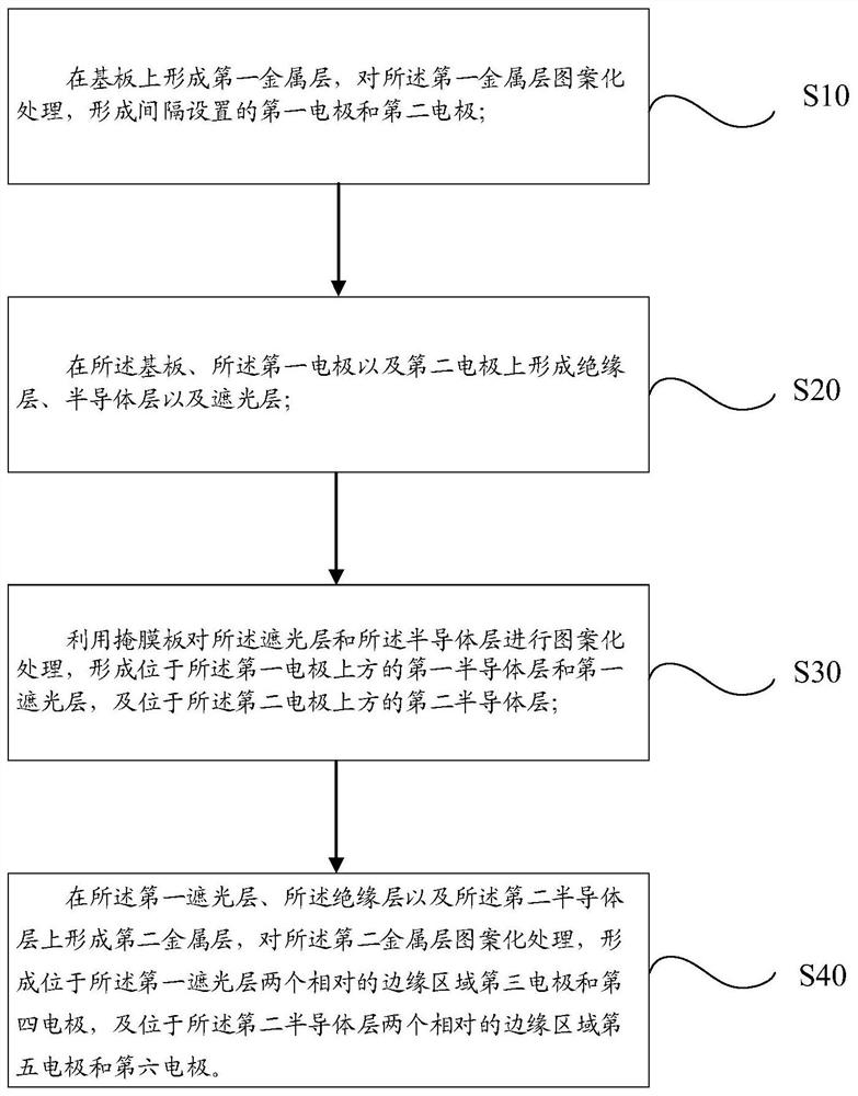
Figure 1 
Figure 2 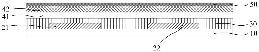
Figure 3
Abstract
Description
technical field
[0001] The present application relates to the field of display technology, in particular to an array substrate and a preparation method thereof. Background technique
[0002] In the field of display technology, driving thin film transistors and sensor thin film transistors are widely used. Sensor thin film transistors require low subthreshold swing, low off-state current density and high electron mobility. In the prior art, indium gallium zinc oxide is usually used The structure of IGZO and indium zinc oxide (IZO) is used as the semiconductor layer of the thin film transistor to meet the above requirements.
[0003] At present, in the in-cell-touch screen, there is a design in which the driving thin film transistor and the sensor thin film transistor are fabricated in the same panel, which requires that the driving thin film transistor should be taken into account when manufacturing. The switching characteristics of the sensor and the photosensitivity of the...
Examples
Embodiment 1
[0051] see figure 1 , a schematic diagram of the process flow of the array substrate provided in the embodiment of the present application.
[0052] In this embodiment, the preparation method of the array substrate includes:
[0053] Step S10: forming a first metal layer on the substrate 10, and patterning the first metal layer to form first electrodes 21 and second electrodes 22 arranged at intervals, such as Figure 2A shown.
[0054]In this embodiment, the step S10 includes the following steps:
[0055] Step S11: providing a substrate 10, the substrate 10 includes but not limited to a glass substrate and a flexible substrate.
[0056] Further, in this embodiment, the substrate 10 is a flexible and transparent PI substrate, mainly polyimide, and the PI material can effectively improve light transmittance.
[0057] Step S12: Depositing a first metal layer on the substrate 10, the material of the first metal layer includes but not limited to metals such as aluminum, molybd...
Embodiment 2
[0094] see image 3 , a schematic structural diagram of the array substrate provided in the embodiment of the present application.
[0095] In this embodiment, the array substrate includes a substrate 10; a switch thin film transistor 100, the switch thin film transistor 100 is arranged in an array on the substrate 10, and the switch thin film transistor 100 includes a stacked first electrode 21 and a The first semiconductor layer 401; the photosensitive thin film transistor 200, the photosensitive thin film transistor 200 is arranged on the substrate 10, the photosensitive thin film transistor 200 includes the second electrode 22 and the second semiconductor layer 402 arranged in a stack; wherein, the photosensitive thin film transistor 200 The switching thin film transistor 100 is spaced apart from the photosensitive thin film transistor 200 , and the switching thin film transistor 100 further includes a light shielding layer 50 located above the first semiconductor layer. ...