

Emitter coupled logic circuit having data heavy dnty function
An emitter-coupled, logic circuit technology, applied in logic circuits, logic circuits using specific components, logic circuits using semiconductor devices, etc., can solve the data reload speed delay, design complexity, affect ECL circuit data reload Operation speed, etc.
Patent Information
- Authority / Receiving Office
- CN · China
- Patent Type
- Patents(China)
- Current Assignee / Owner
- Publication Date
- 2006-09-27
- Estimated Expiration
- Not applicable · inactive patent
Smart Images
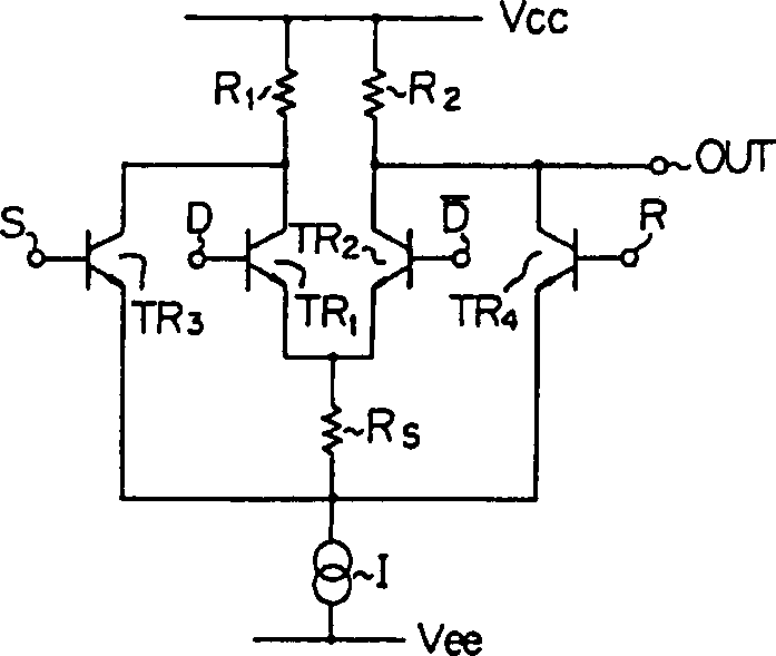
Figure 1 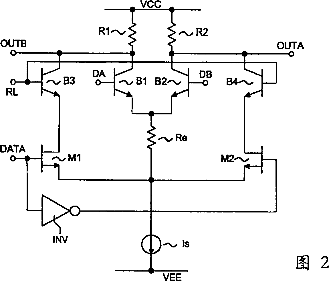
Figure 2 
Figure 3
Abstract
Description
Technical field
[0001] The present invention relates to an emitter coupled logic (Emitter Couple Logic, ECL) circuit, in particular to an emitter coupled logic circuit with a data reload function using a metal oxide semiconductor field effect (MOSFET) transistor. Background technique
[0002] Due to the fast operating speed of emitter coupled logic (hereinafter referred to as ECL) circuits, ECL circuits have been widely used in logic gate circuits, such as Flip-Flops. figure 1 Shown is the ECL circuit "ECL circuit for forcibly setting a high level output" of U.S. Patent No. 4,546,272. The ECL circuit includes a pair of emitter-coupled bipolar transistors TR1 and TR2 for receiving differential signals and load resistors R1, R2, and a resistor R connected to the emitters of the bipolar transistors TR1 and TR2. s , One connected to resistor R s A current source of, and a pair of bipolar transistors TR3 and TR4 for receiving set or reset signals.
[0003] This traditional ECL circuit...
Examples
Embodiment Construction
[0011] Hereinafter, the ECL circuit with data reloading of the present invention will be described in detail with reference to the drawings.
[0012] Figure 2 is an ECL circuit with data reload function of the present invention. As shown in the figure, the ECL circuit of the present invention includes a pair of differential emitter-coupled bipolar transistors B1, B2, a pair of load resistors R1, R2, a pair of heavy-duty control bipolar transistors B3, B4, and a connection A resistor Re at the emitter of the bipolar transistor pair B1, B2, a current source Is connected to the resistor Re, a pair of field effect transistors M1, M2 for receiving heavy load data, and an inverter INV.
[0013] The collectors of the emitter-coupled bipolar transistor pair B1 and B2 are connected to the high working voltage VCC via resistors R1 and R2, and the bases receive the differential signals DA and DB respectively. The emitters of the emitter-coupled bipolar transistor pair B1 and B2 are connected...