
Digital filter design method and device, digital filter design program, and digital filter
A technology of digital filter and design method, applied in the direction of digital technology network, impedance network, electrical components, etc., can solve the problems of heavy processing load, complex and random coefficient values, huge calculation amount, etc., to reduce the number of circuit components and reduce the calculation load and power consumption reduction effect
Patent Information
- Authority / Receiving Office
- CN · China
- Patent Type
- Applications(China)
- Current Assignee / Owner
- Publication Date
- 2005-12-07
- Estimated Expiration
- Not applicable · inactive patent
Smart Images
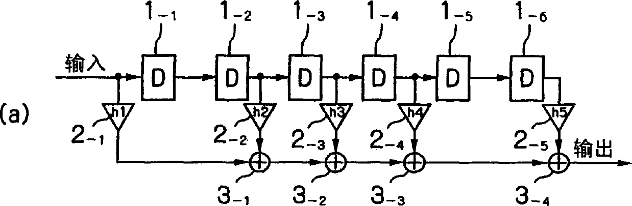
Figure 1 
Figure 2 
Figure 3
Abstract
Description
technical field
[0001] The present invention relates to a design method and device of a digital filter, a program for designing a digital filter, and a digital filter, in particular to a delay line with taps composed of a plurality of delayers, and the signals of each tap are transformed into After several times, the FIR filter and its design method are output after addition. Background technique
[0002] Some kind of digital signal processing is often performed inside various electronic devices used in various fields such as communication, measurement, audio, video signal processing, medical treatment, and seismology. Among the most important basic operations of digital signal processing, there is filtering processing to extract only necessary signals in a certain frequency band from an input signal mixed with various signals or noise. Therefore, digital filters are often used in electronic equipment that performs digital signal processing.
[0003] As a digital filter, a...
Examples
no. 1 Embodiment approach
[0045] In the filter design method of the first embodiment, unit filters L1n" and H1n" (basic filters of the present invention) described below are produced, and an FIR filter with desired frequency characteristics can be designed using only one of them. . In addition, the word "n" appended after the symbol representing the unit filter is the number of clocks representing the delay inserted between the taps, that is, the number of "0"s inserted between the coefficients of each filter (details will be described later). ).
[0046] First, the 5-tap unit filters L1n, H1n serving as a reference for understanding the above-mentioned unit filters L1n", H1n" will be described. FIG. 1 is a diagram showing 5-tap unit filters L10 and H10, (a) showing its circuit configuration, and (b) showing a numerical string of filter coefficients.
[0047]As shown in Figure 1(a), the 5-tap unit filter L10, H10 is a cascaded connection of 6 D-type flip-flops 1 -1 ~1 -6 , delaying the input signal...
no. 2 Embodiment approach
[0132] Next, a second embodiment of the present invention will be described. Figure 22 shows the above-mentioned low-pass filter {1L(2.6)10*2L(2.6)10} 64 The figure, (a) shows its circuit structure, (b) shows the clock used.
[0133]The low-pass filter shown in FIG. 22 has: D-type flip-flops 51 and 56 that operate according to the reference clock CK; D-type flip-flops 53 and 4-stage processing units 54 that operate according to the clock 16CK with a 16-fold frequency; and, according to The multiplexer switch 52 and the data selector 55 are operated by the clock CK1 of 1 / 16 times frequency. The above-mentioned 4-stage processing section 54 is composed of a low-pass filter {1L (2.6) 116*2L (2.6) 116} 4 constitute.
[0134] The data input to the first-stage D-type flip-flop 51 is input to the terminal A side of the multiplexer switch 52 . The data of the low-pass filter processing result output from the terminal B of the data selector 55 is input to the terminal B side of the...