
Image processing chip test method
a technology of image processing and test method, applied in the direction of instruments, static indicating devices, etc., can solve the problems of serious problems that can be found, and achieve the effect of accurately and automatically and accurately detected
Patent Information
- Authority / Receiving Office
- US · United States
- Patent Type
- Patents(United States)
- Current Assignee / Owner
- Publication Date
- 2021-12-14
Smart Images
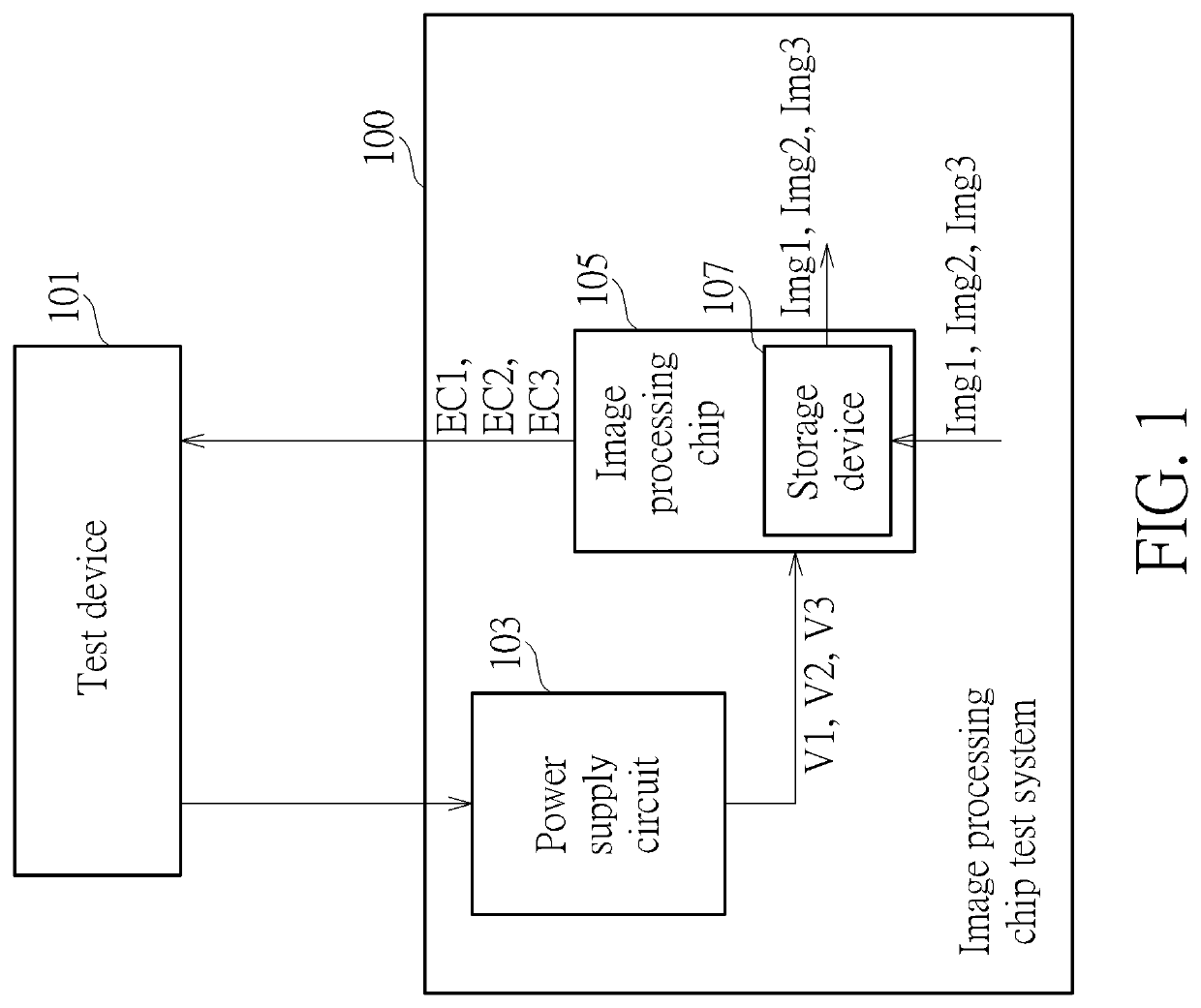
Figure 1 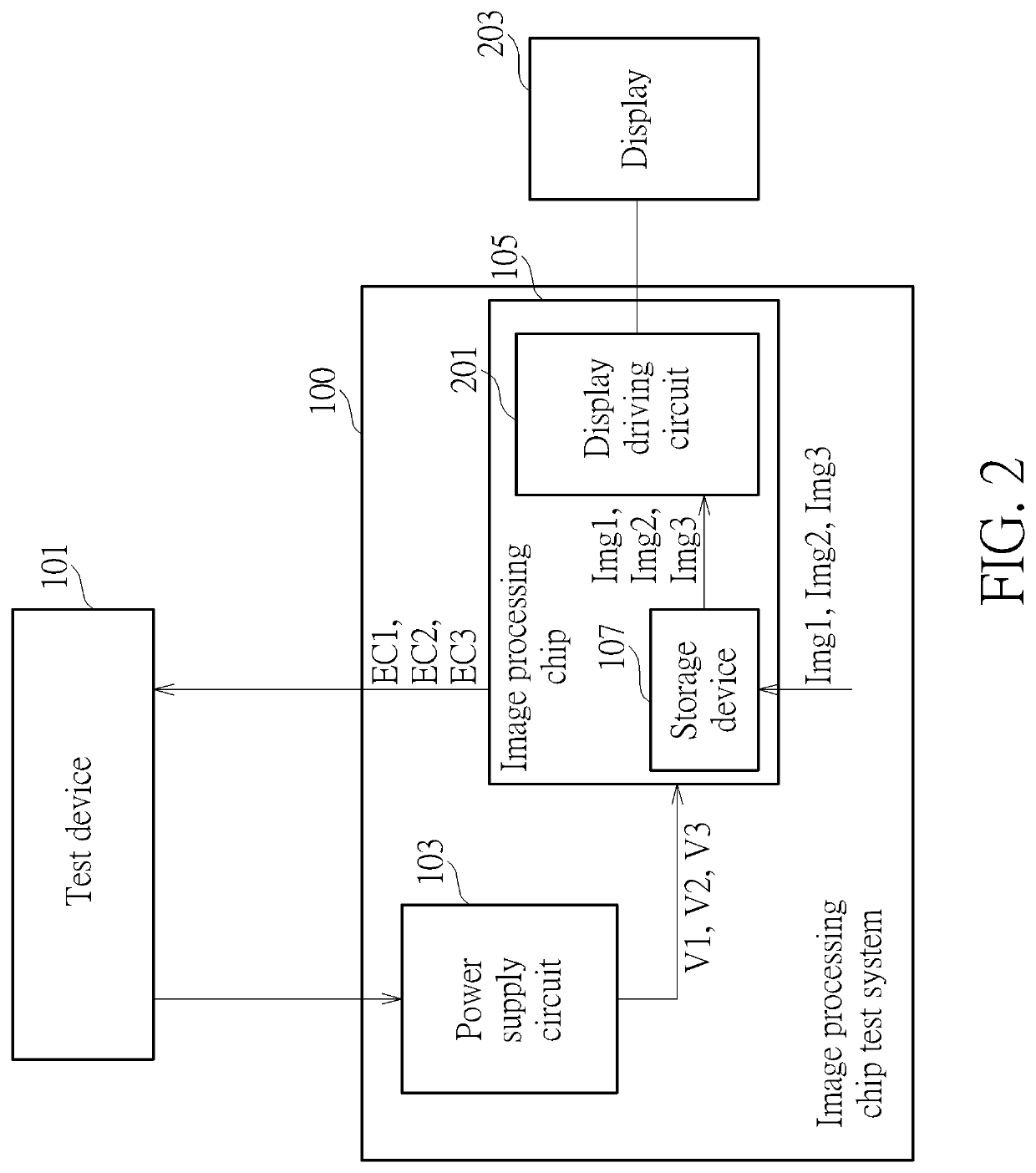
Figure 2 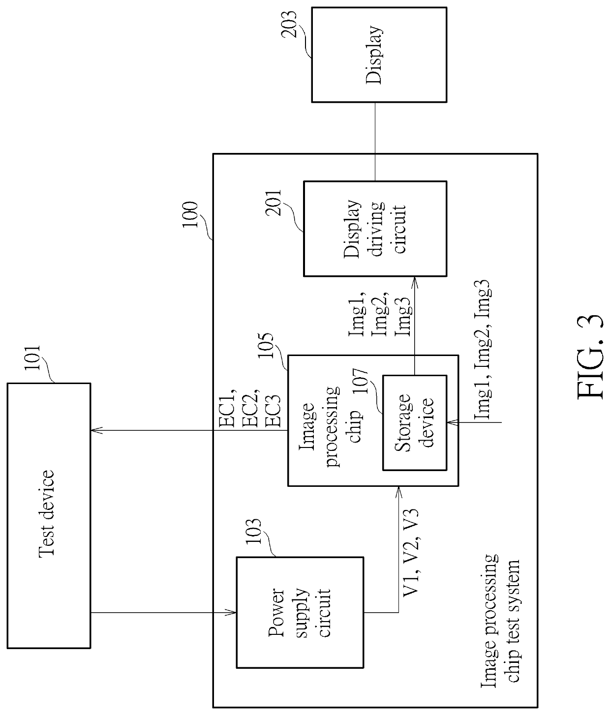
Figure 3
Abstract
Description
BACKGROUND OF THE INVENTION1. Field of the Invention
[0001] The present invention relates to an image processing chip test method, and particularly relates to an image processing chip test method which can automatically test an erroneous operating voltage of an image processing chip.2. Description of the Prior Art
[0002] Conventionally, am operating voltage provided to an image processing chip is manually adjusted when a test of the image processing chip is performed. Also, a display connected to the image processing chip is monitored to see if any problem occurs on the display, such as flashing or image string, to determine whether the operating voltage is proper or not.
[0003] However, only serious problems can be found by such method. If the display only has slight problems, the tester may not find the operating voltage is wrong since the image with problems may not obvious or only shows up in a very short time.SUMMARY OF THE INVENTION
[0004] One objective of the present invention is to ...
Examples
Embodiment Construction
[0014]Several embodiments are provided in following descriptions to explain the concept of the present invention. Each component in following descriptions can be implemented by hardware (e.g. a device or a circuit) or hardware with software (e.g. a program installed to a processor). Besides, the method in following descriptions can be executed by programs stored in a non-transitory computer readable recording medium such as a hard disk, an optical disc or a memory. Besides, the term “first”, “second”, “third” in following descriptions are only for the purpose of distinguishing different one elements, and do not mean the sequence of the elements. For example, a first device and a second device only mean these devices can have the same structure but are different devices.
[0015]FIG. 1 is a block diagram illustrating an image processing chip test system using the image processing chip test method according to one embodiment of the present invention. AS shown in FIG. 1, the image process...