
Flat panel display device
Patent Information
- Authority / Receiving Office
- US · United States
- Current Assignee / Owner
- Publication Date
- 2004-09-09
- Estimated Expiration
- Not applicable · inactive patent
Smart Images
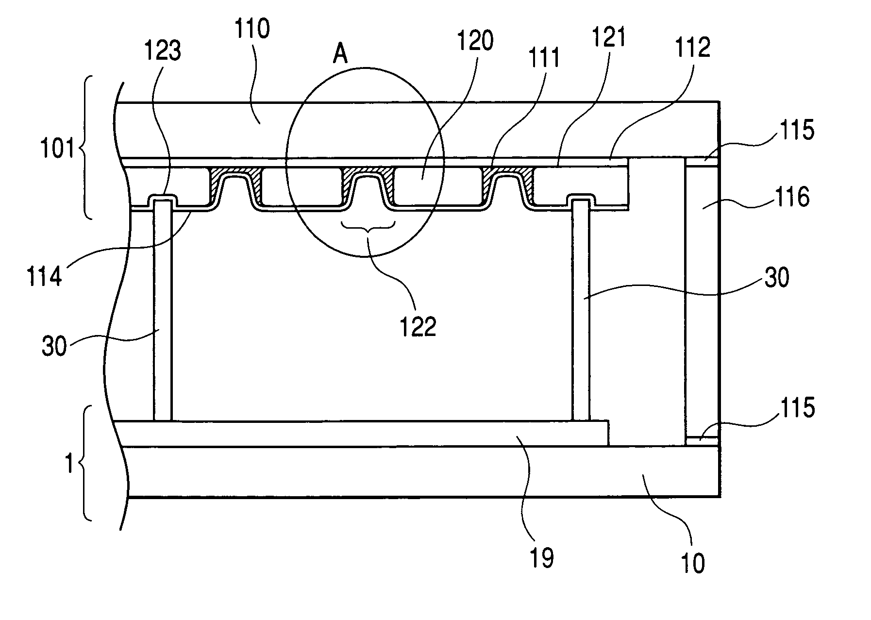
Figure 1 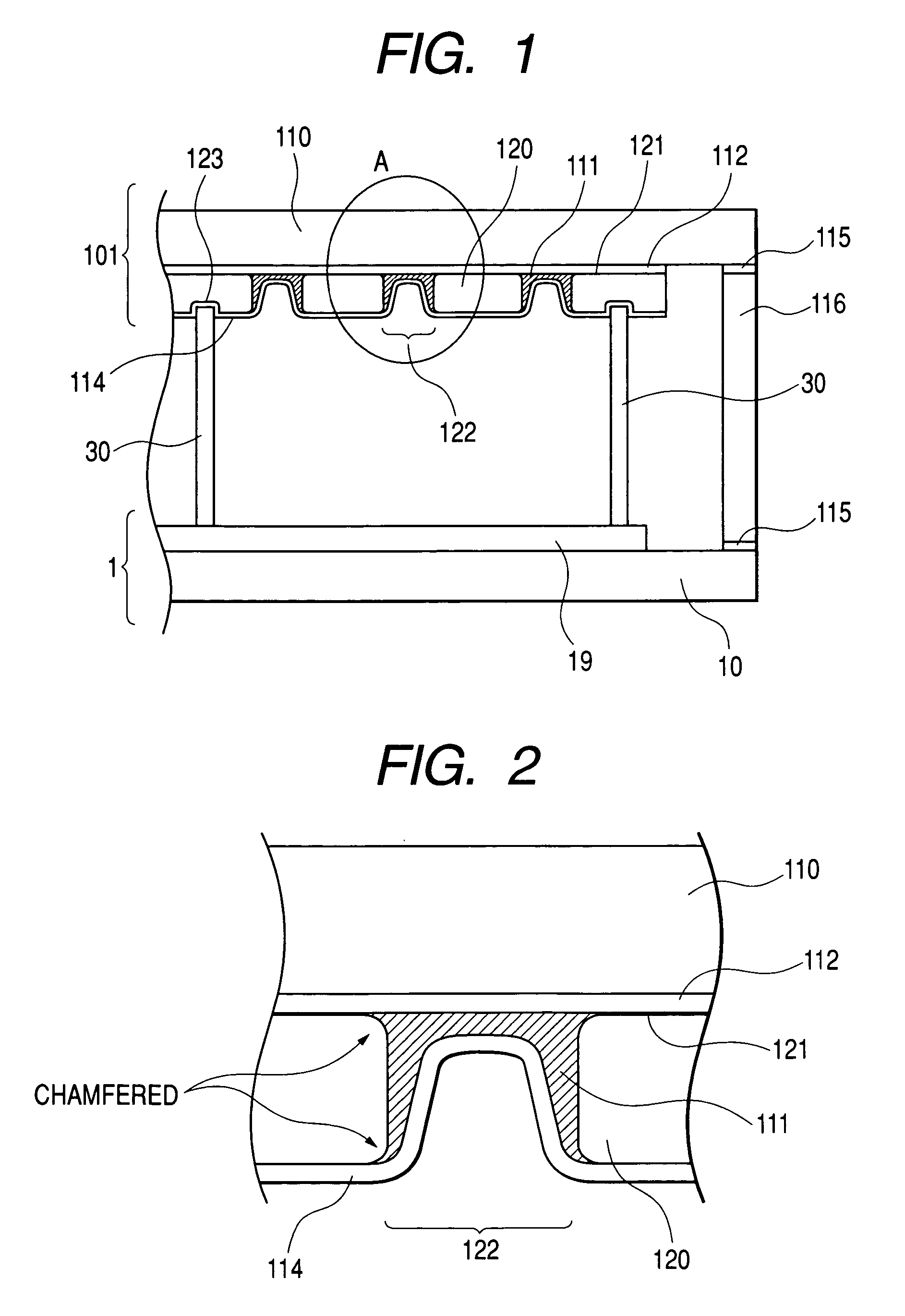
Figure 2 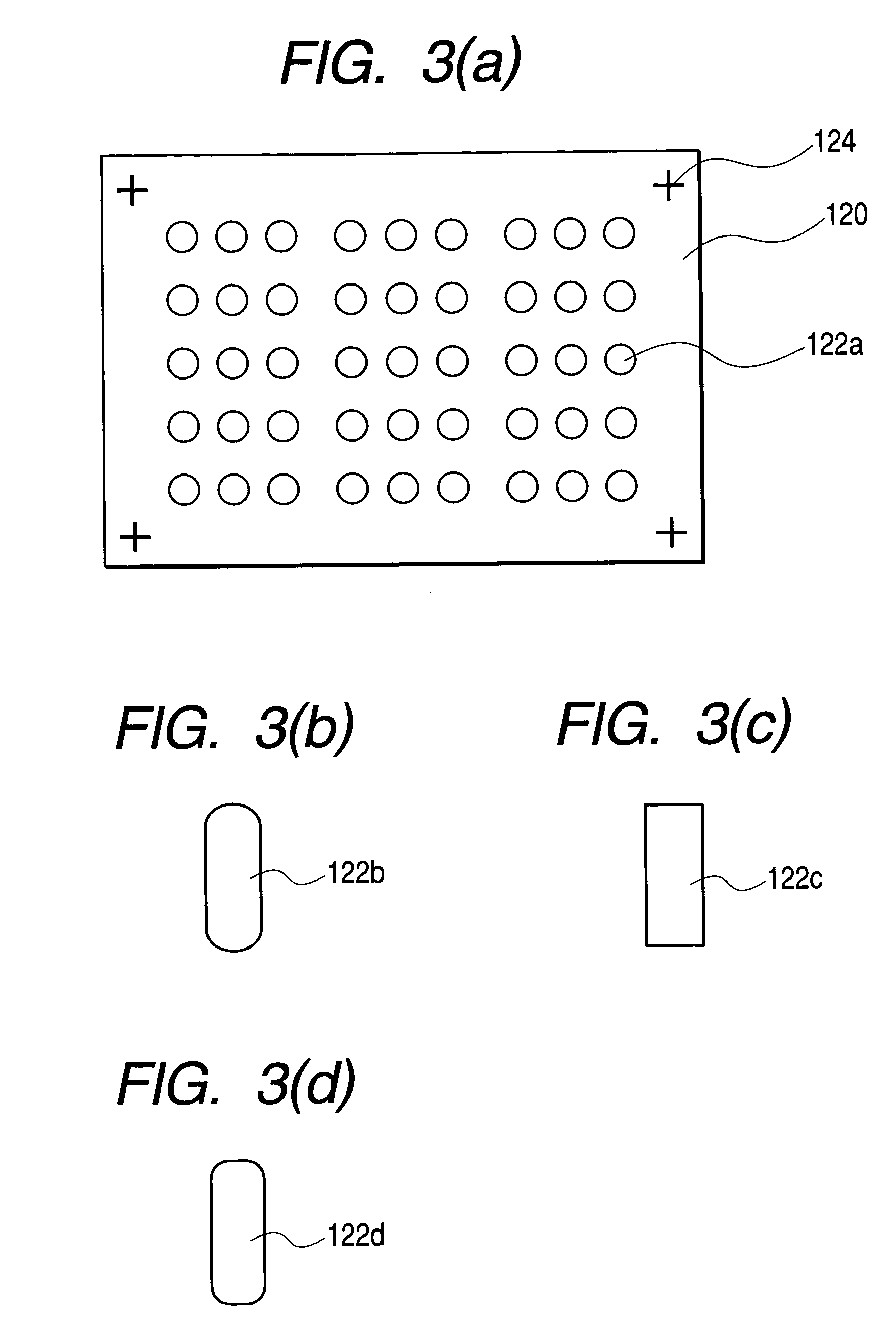
Figure 3
Abstract
Description
2. BACKGROUND OF THE INVENTION
[0001] The present invention relates to a flat panel display device, and in particular to a field emission display (hereinafter FED), a flat panel display device incorporating in a hermetic container an electron source comprising a large number of cold cathode elements arranged in a matrix configuration for emitting electrons.
[0002] Known as electron emitting elements for use in FED are surface conduction type emission element (hereinafter SED type), field emission type (hereinafter FE type) and metal-insulator-metal type emission element (hereinafter MIM type). Among the FE type, there are the Spindt type made up chiefly of a metal such as Mo and a semiconductor material such as Si and the CNT (Carbon Nanotube) type using carbon nanotubes as its electron source. The SED type is disclosed in Japanese Patent Application Laid-Open No. 2000-164129, for example, and the MIM type is disclosed in Japanese Patent Application Laid-Open Nos. 2001-101965 and 2001...
Examples
Embodiment Construction
[0019] The preferred embodiments in accordance with the present invention will be explained by reference to the drawings.
[0020] The following will explain examples of a flat panel display device of the present invention will be explained in detail by reference to FIGS. 1-5(c).
[0021] FIG. 1 illustrates a schematic configuration of a flat panel display device in accordance with an embodiment of the present invention. FIG. 2 is an enlarged detailed view of a portion designated A of FIG. 1. FIG. 3(a) is a top view of a metal sheet, and FIGS. 3(b)-3(d) are plan views of other examples of the shape of fine holes in the metal sheet, respectively. FIGS. 4(a)-4(c) illustrate examples of a metal sheet provided with recesses, FIG. 4(a) is a top view of one of the examples, FIG. 4(b) is a cross-sectional view of the metal sheet of FIG. 4(a), and FIG. 4(C) is a top view of the other examples of the two. FIGS. 5(a) and 5(b) are top views of other two examples of a metal sheet provided with recess...