
Optical head apparatus and optical information processing apparatus
a head apparatus and head technology, applied in the field of optical head apparatus and optical information processing apparatus, can solve the problems of increasing the effective diameter of the necessary optical element, requiring a far greater positive power, and unable to obtain sufficient characteristics and accuracy, so as to reduce the length of the optical path of the entire optical system, the effect of reducing the length of the optical path and ensuring the working distan
Patent Information
- Authority / Receiving Office
- US · United States
- Patent Type
- Applications(United States)
- Current Assignee / Owner
- Publication Date
- 2005-03-03
- Estimated Expiration
- Not applicable · inactive patent
Smart Images
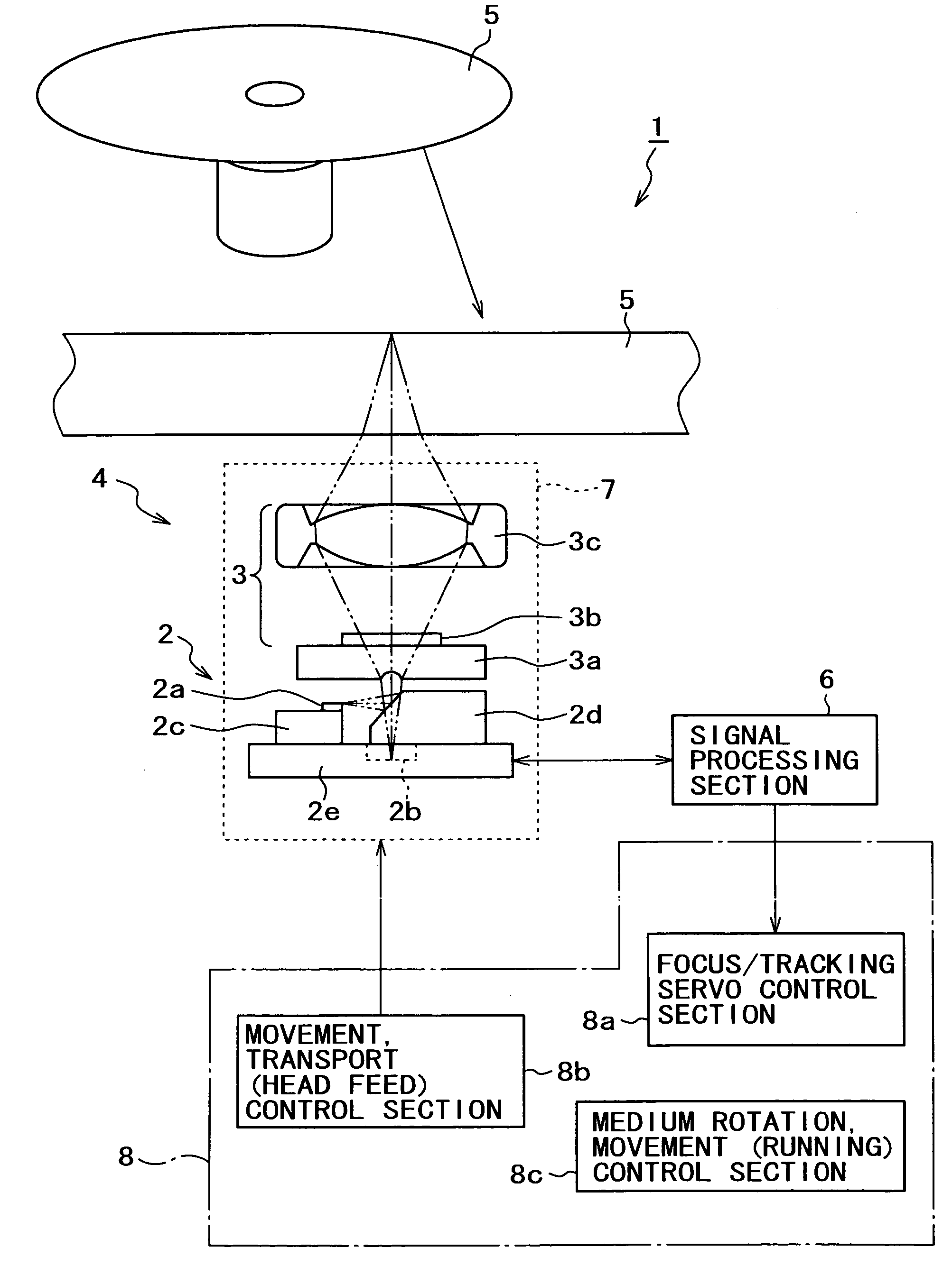
Figure 1 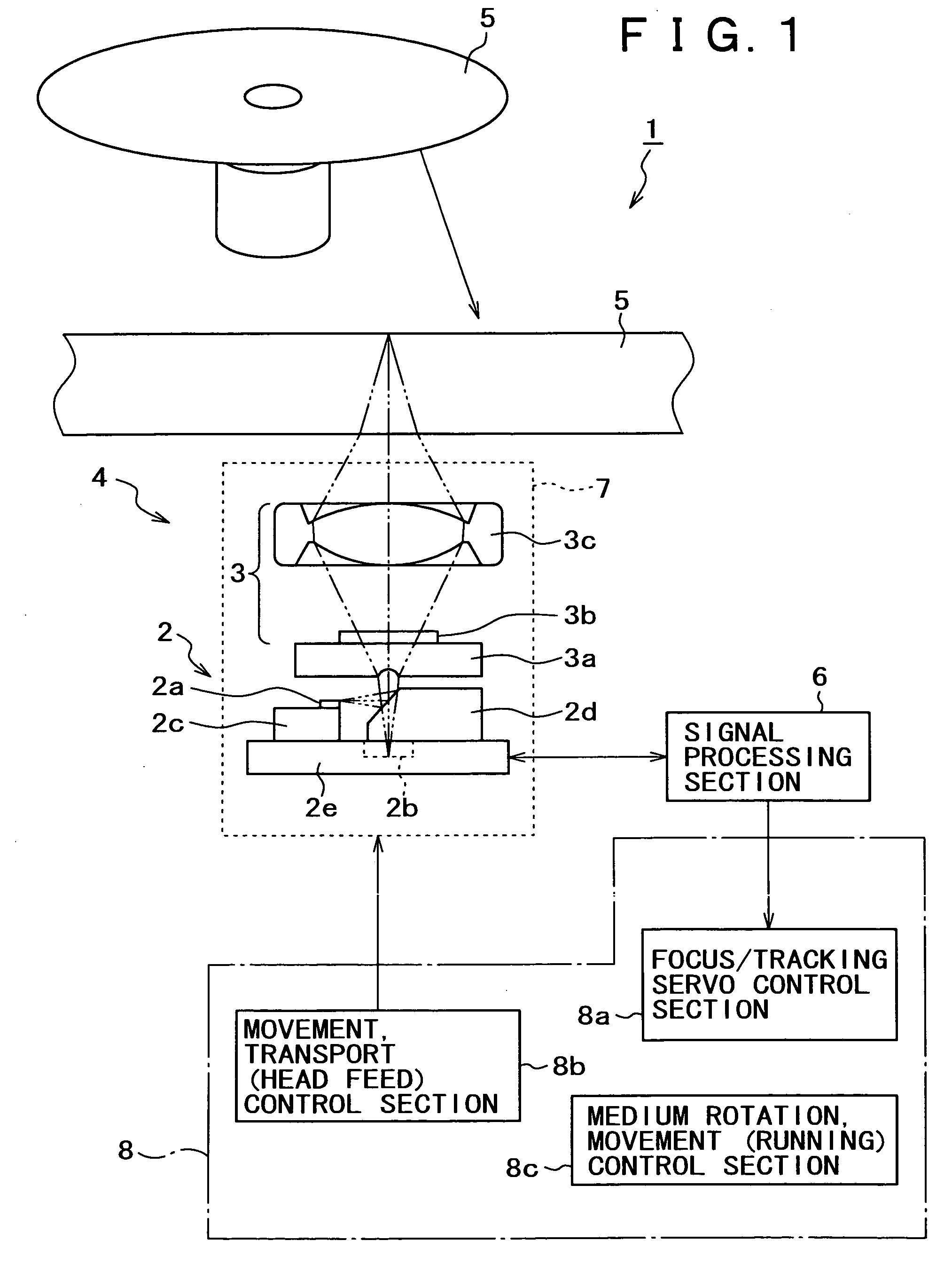
Figure 2 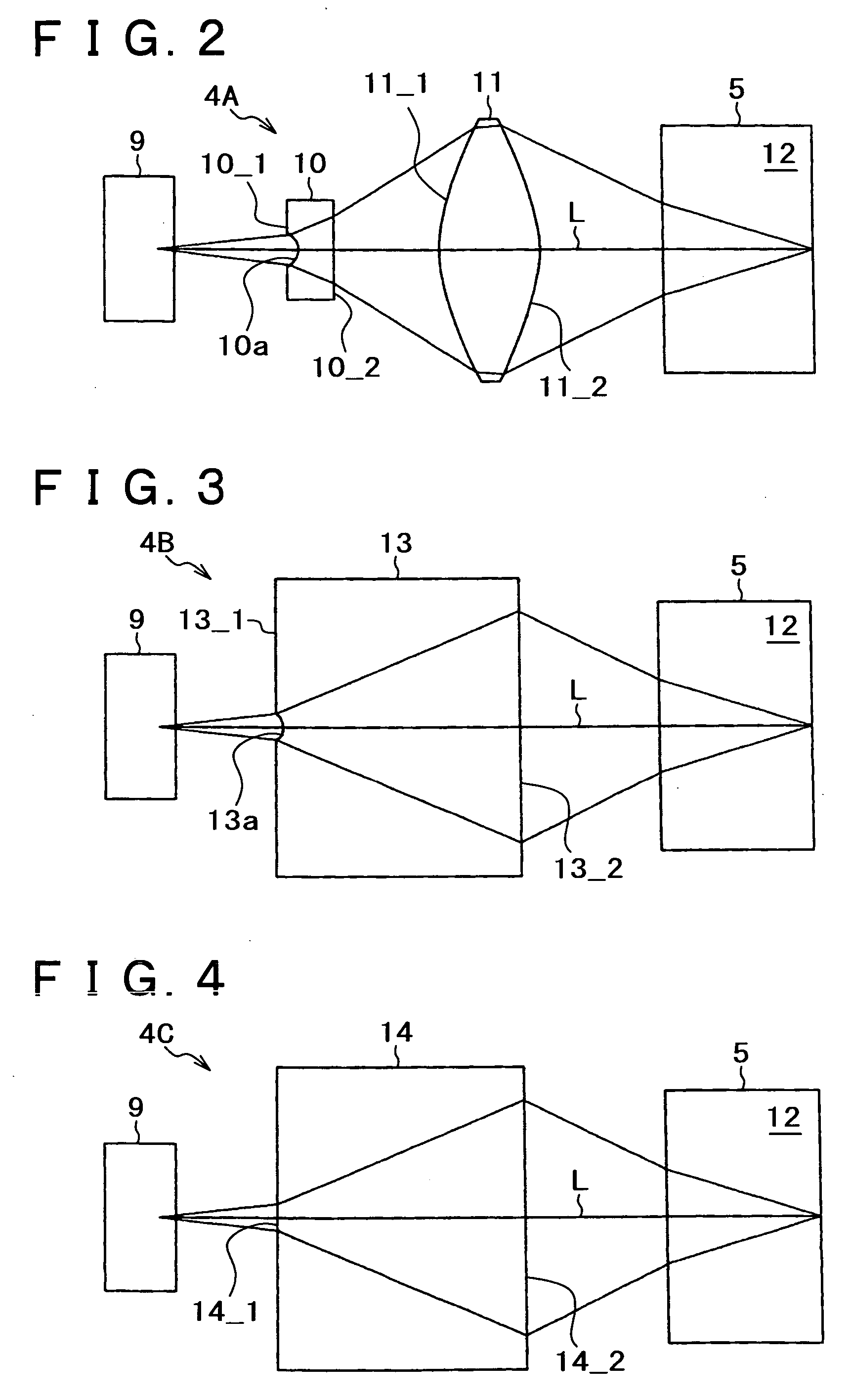
Figure 3
Abstract
Description
CROSS REFERENCE TO RELATED APPLICATION
[0001] The present document is based on Japanese Priority Document JP2003-291310, filed in the Japanese Patent Office on Aug. 11, 2003, the entire contents of which being incorporated herein by reference. BACKGROUND OF THE INVENTION
[0002] 1. Technical Field
[0003] The present invention relates to a technique for reducing an optical path length in an optical system for performing reading or recording of information by making use of light irradiation onto an optical recording medium.
[0004] 2. Description of Related Art
[0005] An optical head apparatus (such as an optical pickup apparatus) to be used for the reproduction and recording of information associated with an optical disk is provided with, for example, a light source such as a laser diode, lens elements (such as a collimator lens and a coupling lens) which convert light scattered from the light source into an approximately parallel light beam, and an objective lens which condenses the l...
Examples
embodiment 1
[0042]FIG. 2 shows the essential portion of an optical system associated with the above-mentioned form (I), and in FIG. 2, “L” denotes its optical axis.
[0043] In an optical system 4A shown in this embodiment, a composite element (a so-called laser coupler) of a laser diode and a photodetector is used as a light-emitting / receiving element (or a light-transmitting / receiving element) 9, and light exiting from the composite element, after having been transmitted through a coupling lens 10, is irradiated onto an optical disk 12 (part of which is shown in FIG. 2) via an objective lens 11.
[0044] The coupling lens 10 disposed near the light-emitting / receiving element 9 has negative power as a whole. In this embodiment, a concave surface 10a is formed on a first surface 10_1 opposed to the light-emitting / receiving element 9, and a second surface 10_2 on the side of an optical disk 12 is formed as a plane surface. Incidentally, the concave surface 10a is formed as an aspherical surface havi...
embodiment 2
[0049]FIG. 3 shows the essential portion of an optical system associated with the above-mentioned form (II), and “L” denotes its optical axis.
[0050] In an optical system 4B shown in this embodiment, the light-emitting / receiving element 9 which is the same as that of Embodiment 1 is used, and light exiting therefrom, after having been transmitted through a hologram element 13, is irradiated onto the optical disk 12.
[0051] In the hologram element 13, a first surface 13_1 opposed to the light-emitting / receiving element 9 has negative power, and a concave surface 13a is formed as an aspherical surface of negative curvature. A second surface 13_2 opposed to the optical disk 12 is formed as a hologram surface having positive power. Namely, in this embodiment, positive power is obtained only from the surface on which the hologram pattern is formed on a plane surface, whereby the optical path length of the entire system can be made short.
[0052] Since the first surface having negative pow...
embodiment 3
[0053]FIG. 4 shows the essential portion of an optical system associated with the above-mentioned form (II), and in FIG. 4, “L” denotes its optical axis.
[0054] An optical system 4C shown in this embodiment differs from the optical system 4B shown in Embodiment 2 in that both the first and second surfaces of its hologram element are formed as hologram surfaces.
[0055] Namely, light exiting from the light-emitting / receiving element 9 is irradiated onto the optical disk 12 after having been transmitted through a hologram element 14, and in the hologram element 14, a first surface 14_1 opposed to the light-emitting / receiving element 9 is formed as a hologram surface having negative power, and a second surface 14_2 opposed to the optical disk 12 is formed as a hologram surface having positive power.
[0056] In this embodiment as well, it is advantageous in terms of accuracy and the number of component parts that the first surface having negative power and the second surface having positi...