
Semiconductor optical device on an indium phosphide substrate for long operating wavelengths
a technology of indium phosphide and optical devices, applied in semiconductor lasers, lasers, radiation controlled devices, etc., can solve the problem of not providing useful wavelengths, and achieve the effect of increasing the thermal performance of lasers
Patent Information
- Authority / Receiving Office
- US · United States
- Patent Type
- Applications(United States)
- Current Assignee / Owner
- Publication Date
- 2005-03-17
Smart Images
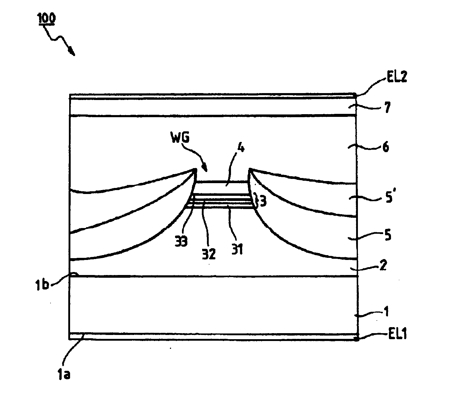
Figure 1 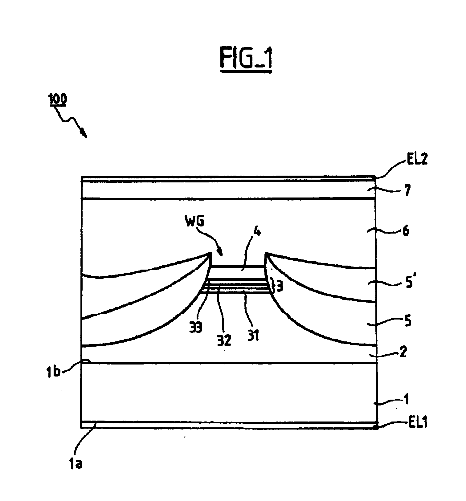
Figure 2 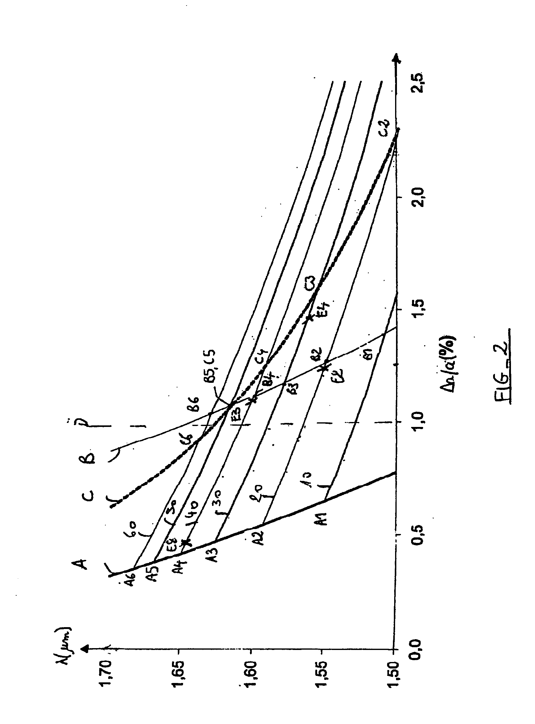
Figure 3
Abstract
Description
CROSS-REFERENCE TO RELATED APPLICATIONS
[0001] This application claims benefit of French Patent Application No. 03 08 770, filed Jul. 18, 2003, which is herein incorporated by reference. BACKGROUND OF THE INVENTION
[0002] 1. Field of the Invention
[0003] The present invention relates to an optical semiconductor device that has a long operating wavelength and comprises an indium phosphide substrate.
[0004] 2. Description of the Related Art
[0005] As is well known, lasers operating at long wavelengths, i.e. above 1.5 μm, are intended to be used for optical data transmission in the so-called C band (1530-1570 nm) and / or the so-called L band (1570-1610 nm).
[0006] These lasers have a vertical structure formed from a stack of semiconductor layers on a semiconductor substrate. In this stack there is an active layer, conventionally with single or multiple quantum wells separated by barrier layers, and interposed between two optical confinement layers.
[0007] The document with the title “Le...
Examples
example 1
[0061] The quantum-well layer is of In0.4Ga0.6As0.995N0.005 with thickness chosen to be 14 nm for example. The operating wavelength is 1.55 μm. The quantum-well layer has a tensile stress of about 1%.
[0062] In the example the barrier layers are of Al0.31In0.69As and of thickness equal to about 10 nm.
example 2
[0063] The quantum-well layer is of In0.38Ga0.62As0.99N0.01 with thickness chosen to be 10 nm for example. The operating wavelength is 1.55 μm. The quantum-well layer has a tensile stress of about 1.25%.
[0064] In the example the barrier layers are of Al0.31In0.69As and of thickness equal to about 10 nm.
example 3
[0065] The quantum-well layer is of In0.4Ga0.6As0.99N0.01 with thickness chosen to be 14 nm for example. The operating wavelength is 1.60 μm. The quantum-well layer has a tensile stress of about 1.1%.
[0066] In the example the barrier layers are of Al0.3In0.69As and of thickness equal to about 10 nm.