
Light-receiving panel or light-emitting panel, and manufacturing method thereof
Patent Information
- Authority / Receiving Office
- US · United States
- Current Assignee / Owner
- Publication Date
- 2006-03-02
- Estimated Expiration
- Not applicable · inactive patent
Smart Images
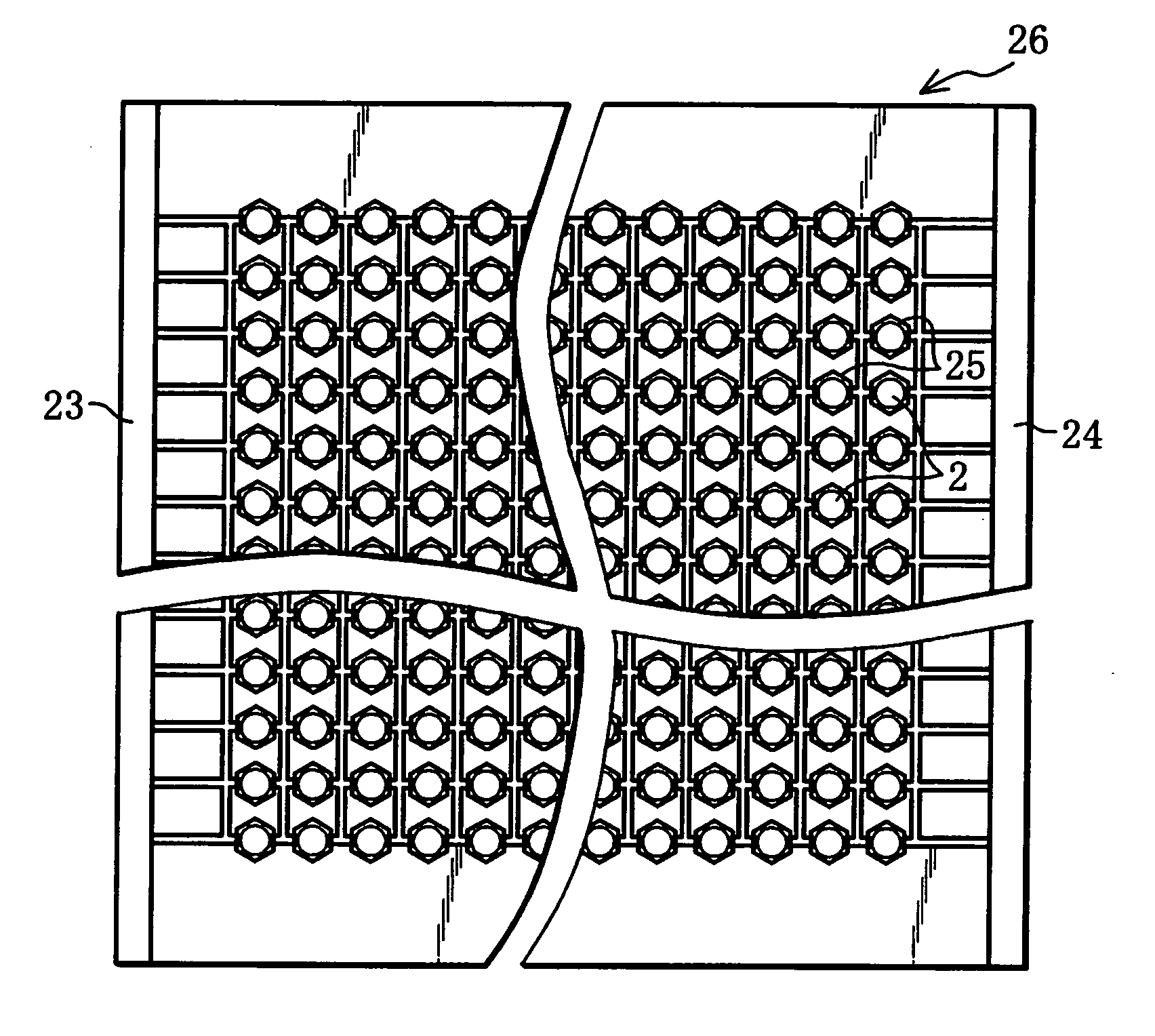
Figure 1 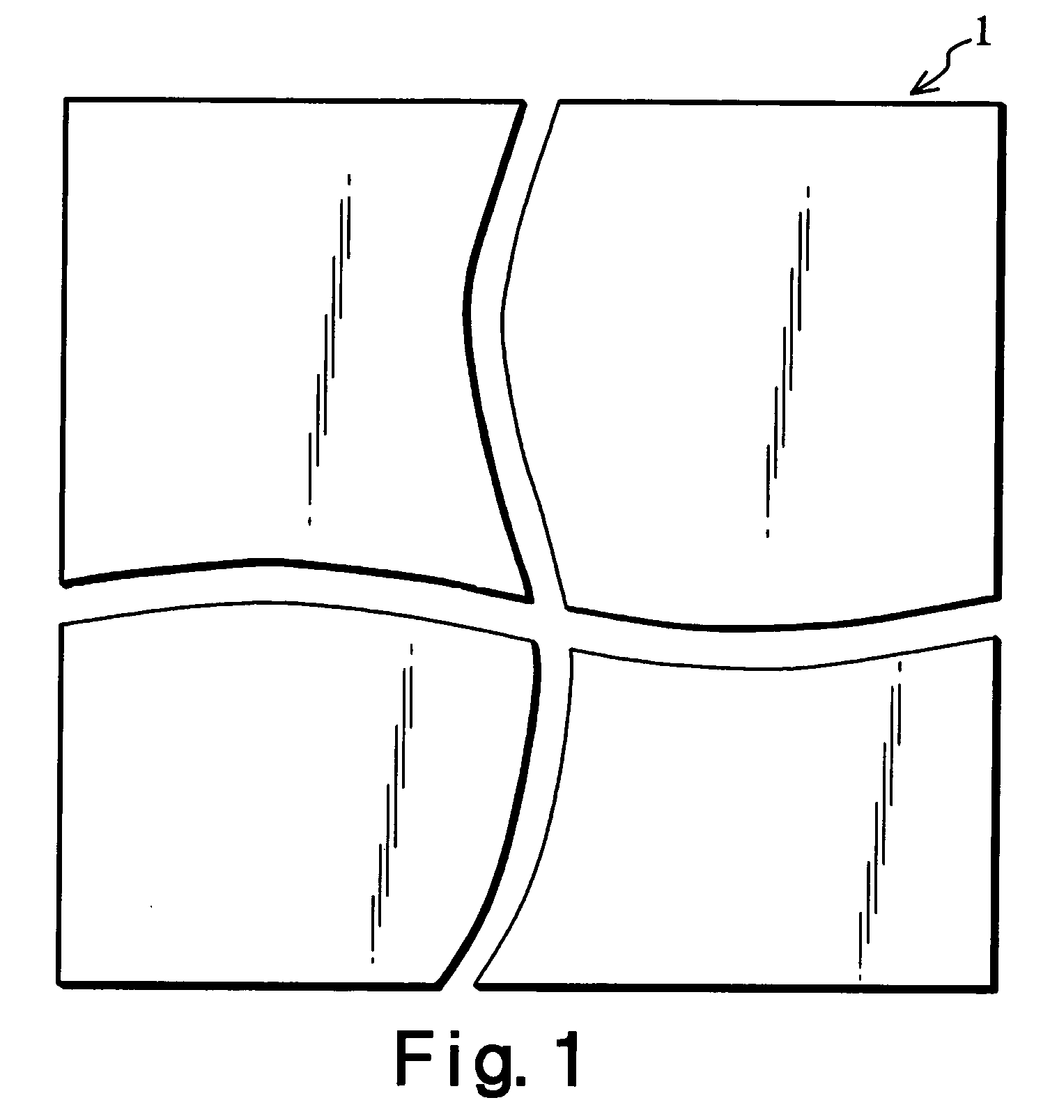
Figure 2 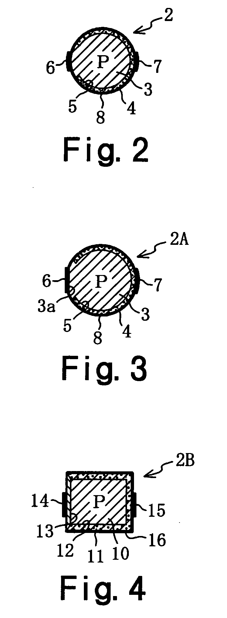
Figure 3
Abstract
Description
TECHNICAL FIELD
[0001] The present invention relates to a light receiving or light emitting panel which can be simply manufactured by mounting light receiving elements or light emitting elements in a plurality of retaining holes formed in a printed wiring sheet, and then sealing these mounted elements with a resin, and a method of manufacturing such a panel. BACKGROUND OF THE INVENTION
[0002] In a conventional solar cell, an n type diffusion layer is formed on the surface of a p type semiconductor substrate, a light receiving surface electrode with a herringbone pattern is formed on the front surface side, a back surface electrode is formed on the back surface side, and the overall device is constructed as a flat-plate panel structure. In such a flat-plate solar cell panel, when the angle of incidence of sunlight increases in the morning and evening, the proportion of reflected light increases, and the proportion of light that enters the panel drops.
[0003] Conventionally, therefore...
Examples
Embodiment Construction
[0060] Embodiments of the present invention will be described below with reference to the attached drawings.
[0061] The present embodiment is an example of a case in which the present invention is applied to a solar cell panel as a light receiving panel. A method for manufacturing this solar cell panel, and the structure of this solar cell panel, will be described.
[0062] First, in a first step, the printed wiring sheet material 1 shown in FIG. 1, and numerous particulate semiconductor elements 2 (3600 elements in the present embodiment, hereafter referred to as “solar cells”) that have a light-to-electricity transducing function, are prepared.
[0063] As is shown in FIG. 1, the printed wiring sheet material 1 is a flat-plate material that is formed by cutting a thin transparent sheet material such as an epoxy type synthetic resin, acrylic type synthetic resin, polyester type synthetic resin, polycarbonate or the like (for example thickness 0.4 to 0.6 mm, 0.6 mm in the present embodi...