
Differential and hierarchical sensing for memory circuits
a memory circuit and hierarchical sensing technology, applied in the field of memory devices, can solve the problems of increasing memory size requirements, exacerbating speed and noise immunity problems, and reducing the design of memory circuit architecture to meet such requirements, so as to improve noise immunity in the memory circuit, reduce latency, and the effect of reducing the electrical load
Patent Information
- Authority / Receiving Office
- US · United States
- Patent Type
- Applications(United States)
- Current Assignee / Owner
- Publication Date
- 2007-02-01
- Estimated Expiration
- Not applicable · inactive patent
Smart Images
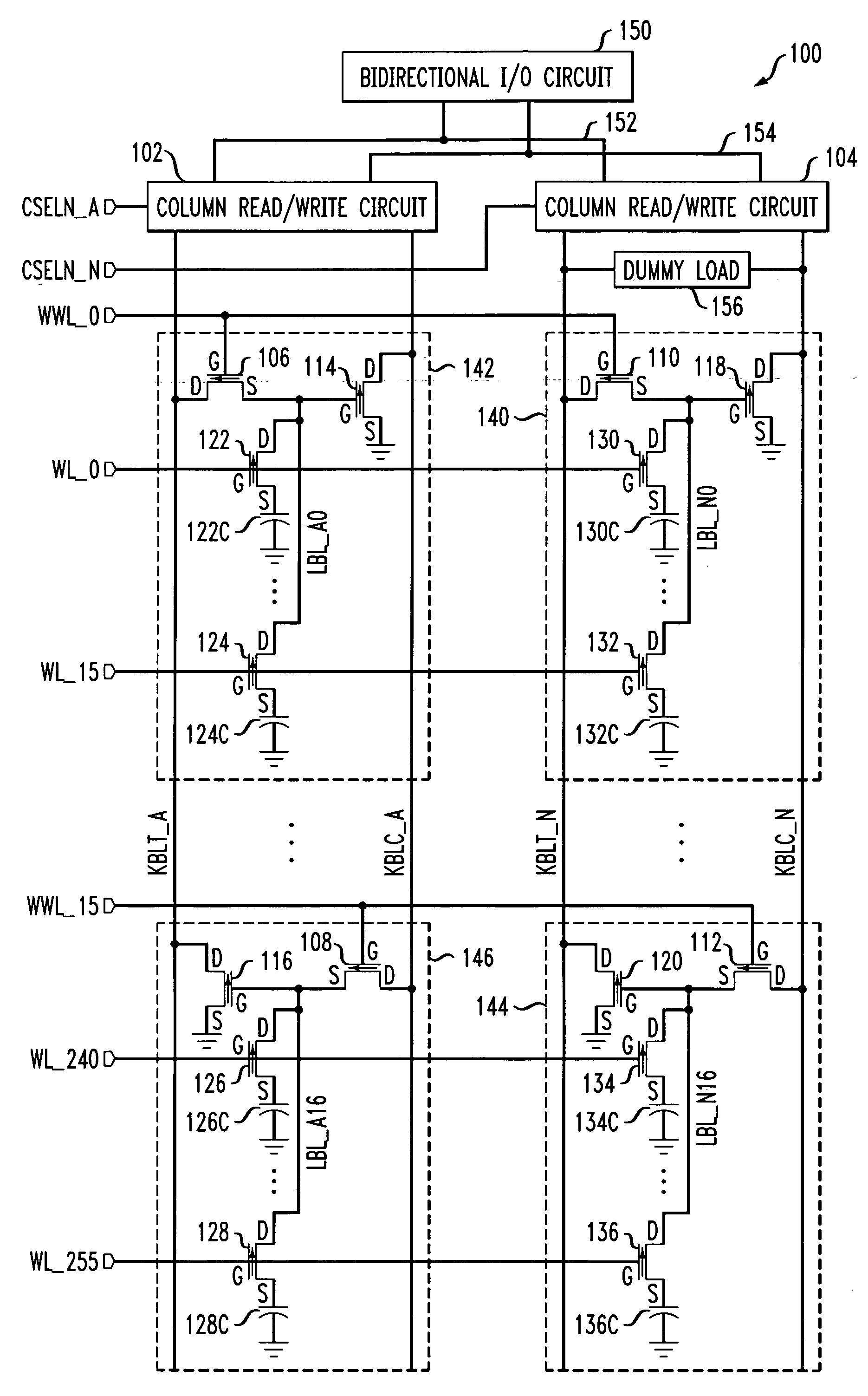
Figure 1 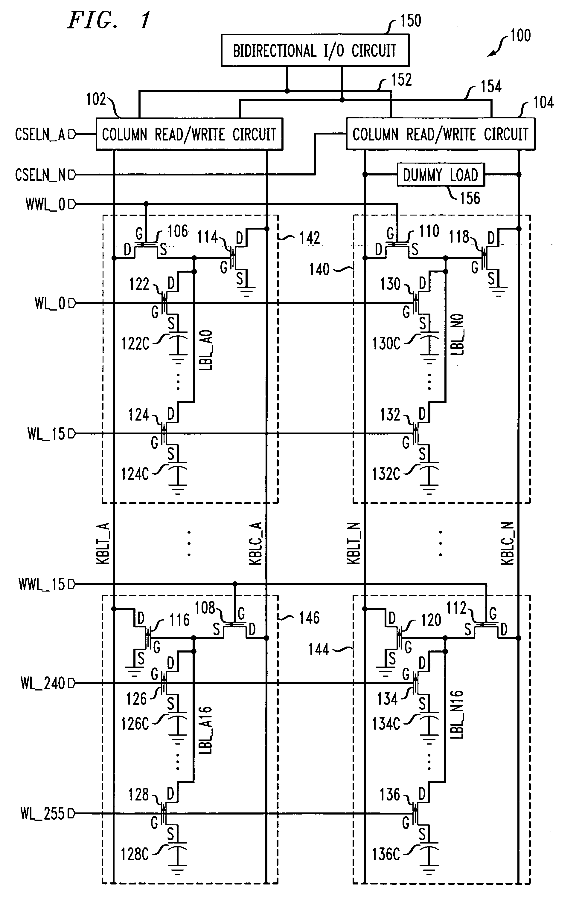
Figure 2 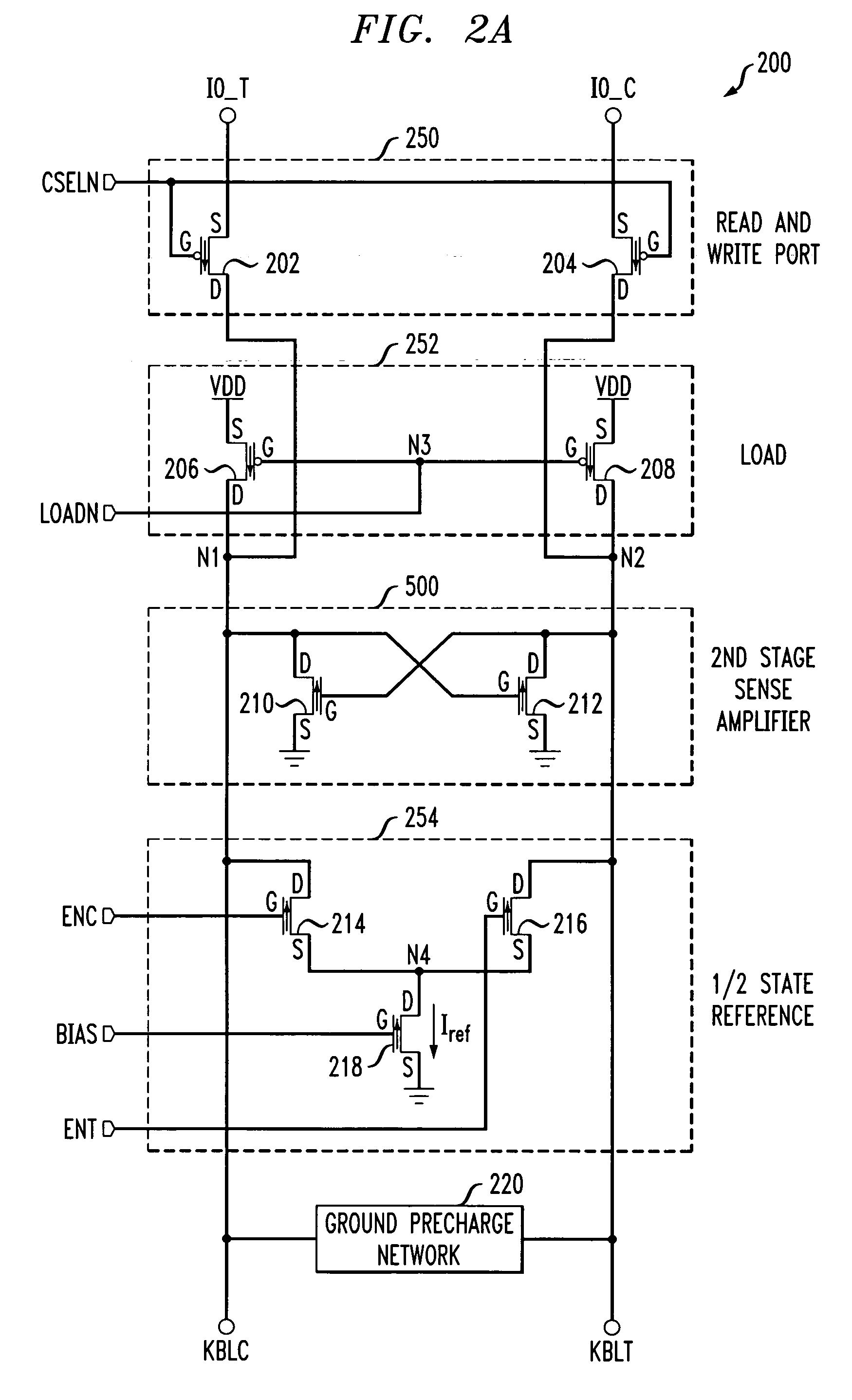
Figure 3
Abstract
Description
FIELD OF THE INVENTION
[0001] The present invention relates generally to memory devices, and more particularly relates to techniques for improving latency and / or noise immunity in a memory circuit. BACKGROUND OF THE INVENTION
[0002] Memory circuits, including, for example, dynamic random access memory (DRAM), are employed in a wide variety of devices and applications. As memory access time requirements are pushed faster and noise immunity requirements are increased, the design of memory circuit architectures to meet such requirements becomes significantly more challenging. Additionally, memory sizes requirements are continuously increasing, thereby exacerbating speed and noise immunity problems.
[0003] Various memory architectures have been proposed to meet certain design criteria, such as, for example, memory access time, often measured as latency. However, although these known memory architectures have had some successes at reducing memory latency, they have often achieved such a ...
Examples
second embodiment
[0061]FIG. 3A is a schematic diagram illustrating at least a portion of an exemplary sense amplifier circuit 300, formed in accordance with the present invention. As apparent from the figure, the sense amplifier circuit 300 is essentially the same as sense amplifier circuit 200 described above in conjunction with FIG. 2A, except that the load 252 in sense amplifier circuit 200 has been modified in sense amplifier circuit 300 to incorporate the functions of the half-state reference generator 254. Specifically, sense amplifier circuit 300 includes a load 301 comprising PMOS transistors 206 and 208, and a switched voltage bias network 302. PMOS transistor 206 includes a source connecting to a first voltage source supplying a first voltage, preferably VDD, a gate for receiving a first bias signal, BIASA, and a drain connected to a complement bank bit line, KBLC, at node N1. PMOS transistor 208 includes a source connecting to VDD, a gate for receiving a second bias signal, BIASB, and a d...
third embodiment
[0066]FIG. 4A is a schematic diagram illustrating at least a portion of an exemplary sense amplifier circuit 400, formed in accordance with the present invention. As apparent from the figure, the sense amplifier circuit 400 is essentially the same as sense amplifier circuit 200 shown in FIG. 2A, except that the load 252 in sense amplifier circuit 200 has again been modified in sense amplifier circuit 400 to incorporate the functions of the half-state reference generator 254, as well as additional features which will be described below. Specifically, sense amplifier circuit 400 includes a load circuit 401 which is operative to provide independent control of the gates of PMOS load devices 206, 208 for the purpose of enabling at least two operational modes, namely, an amplifying mode and a latching mode.
[0067] The load circuit 401 preferably comprises first and second PMOS load devices 206, 208, and a PMOS load enable device 402. A source of each device 206, 208 is connected to a drain...