

Apparatus for thermal and plasma enhanced vapor deposition and method of operating
Patent Information
- Authority / Receiving Office
- US · United States
- Current Assignee / Owner
- Publication Date
- 2007-05-24
- Estimated Expiration
- Not applicable · inactive patent
Smart Images
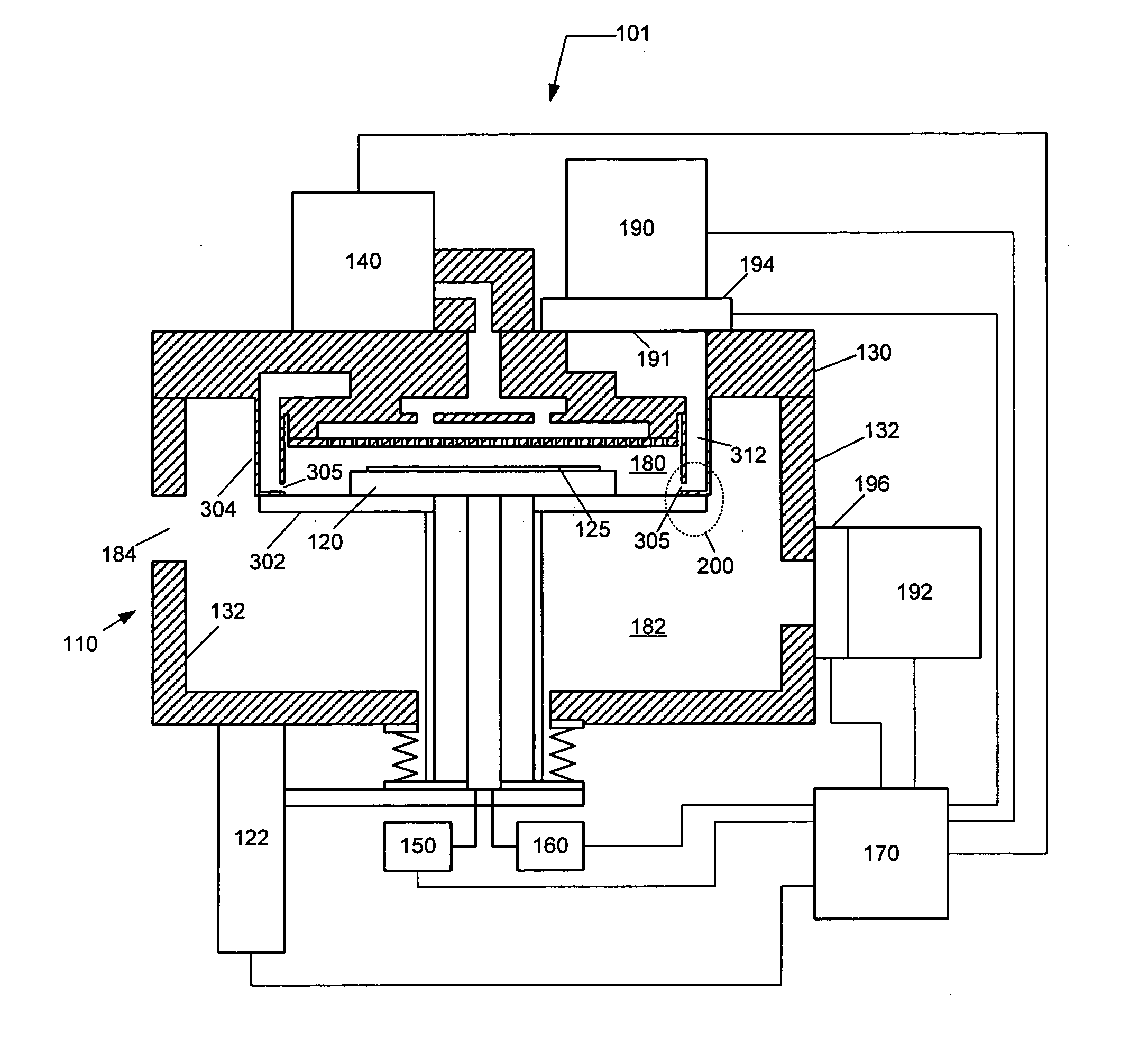
Figure 1 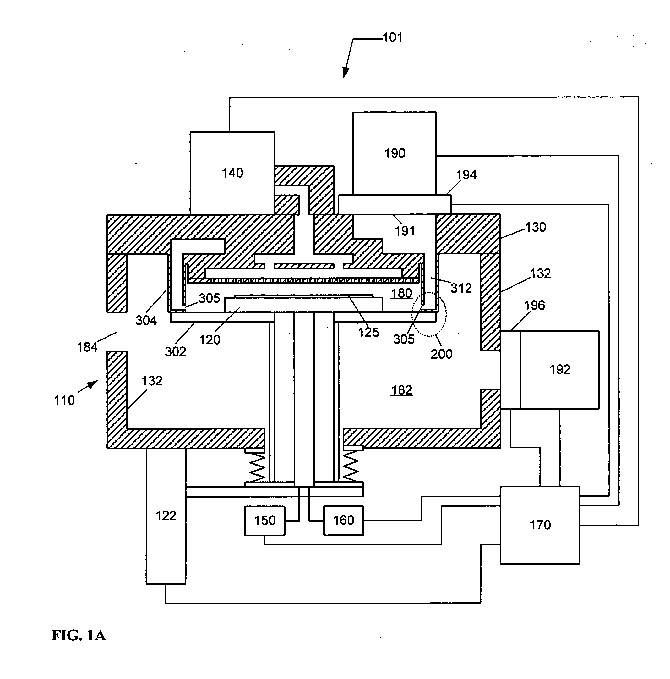
Figure 2 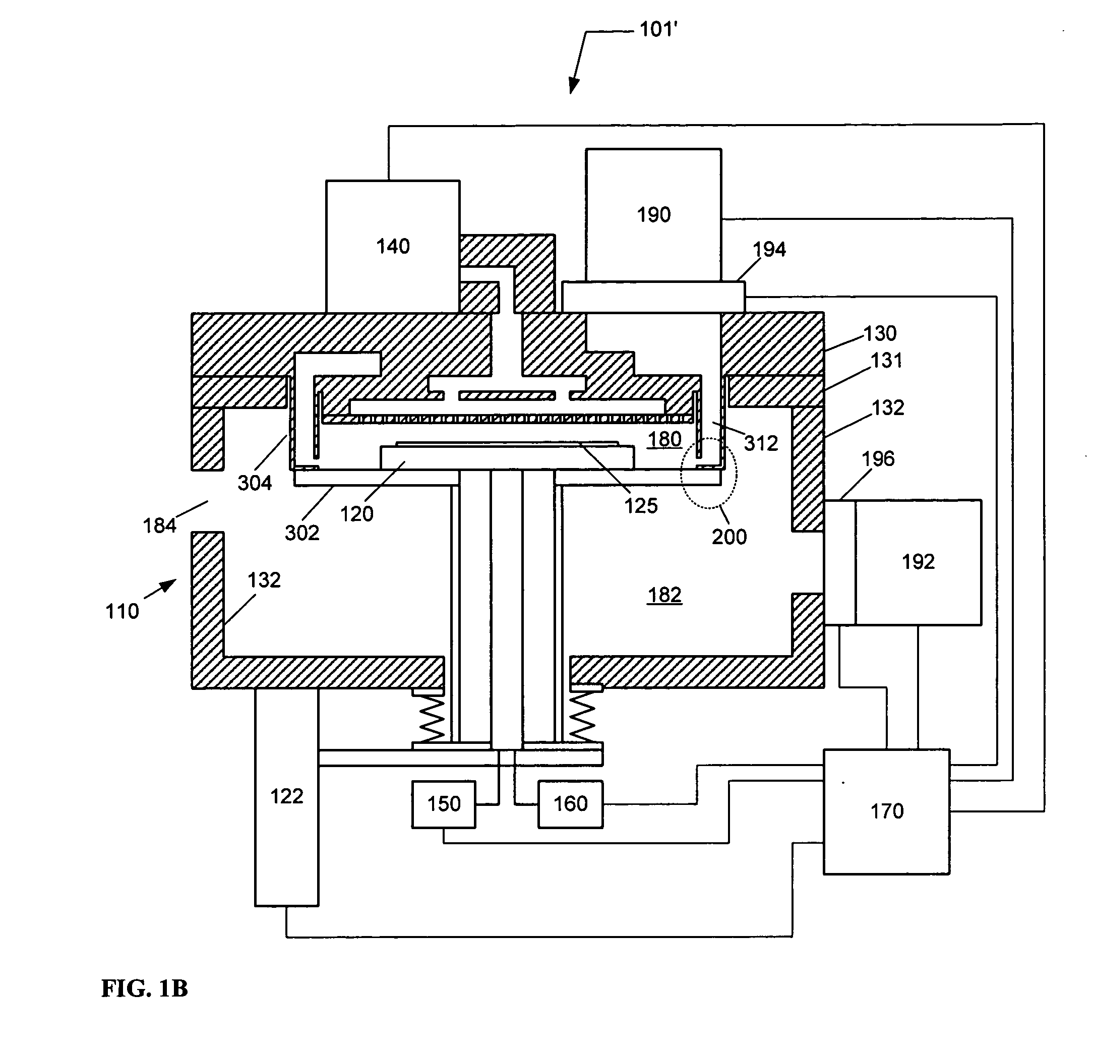
Figure 3
Abstract
Description
CROSS REFERENCE TO RELATED APPLICATIONS
[0001] This application is related to U.S. Ser. No. 11 / 090,255, Attorney Docket No. 26 7366US, Client Ref. No. TTCA 19, entitled “A PLASMA ENHANCED ATOMIC LAYER DEPOSITION SYSTEM”, now U.S. Pat. Appl. Publ. No. 2004VVVVVVVVVV, the entire contents of which are incorporated herein by reference. This application is related to U.S. Ser. No. 11 / 084,176, entitled “A DEPOSITION SYSTEM AND METHOD”, Attorney Docket No. 265595US, Client Ref. No. TTCA 24, now U.S. Pat. Appl. Publ. No. 2004VVVVVVVVVV, the entire contents of which are incorporated herein by reference. This application is related to U.S. Ser. No. XX / XXX,XXX, entitled “A PLASMA ENHANCED ATOMIC LAYER DEPOSITION SYSTEM HAVING REDUCED CONTAMINATION”, Client Ref. No. TTCA 27, now U.S. Pat. Appl. Publ. No. 2004VVVVVVVVVV, the entire contents of which are incorporated herein by reference. This application is related to U.S. Ser. No. XX / XXX,XXX, entitled “METHOD AND SYSTEM FOR PERFORMING THERMAL AN...
Examples
Embodiment Construction
[0022] In the following description, in order to facilitate a thorough understanding of the invention and for purposes of explanation and not limitation, specific details are set forth, such as a particular geometry of the deposition system and descriptions of various components. However, it should be understood that the invention may be practiced in other embodiments that depart from these specific details.
[0023] Referring now to the drawings, wherein like reference numerals designate identical or corresponding parts throughout the several views, FIG. 1A illustrates a deposition system 101 for depositing a thin film, such as for example a barrier film, on a substrate using for example a plasma enhanced atomic layer deposition (PEALD) process. During the metallization of inter-connect and intra-connect structures for semiconductor devices in back-end-of-line (BEOL) operations, a thin conformal barrier layer may be deposited on wiring trenches or vias to minimize the migration of me...