
Rare earth element-doped oxide precursor with silicon nanocrystals
a technology of rare earth elements and precursors, applied in semiconductor/solid-state device manufacturing, basic electric elements, electric devices, etc., can solve the problems of low device efficiency, increased cost, and insufficient interface engineering to support the use of rare earth element-doped oxide precursors, etc., to achieve the effect of reducing production costs
Patent Information
- Authority / Receiving Office
- US · United States
- Patent Type
- Applications(United States)
- Current Assignee / Owner
- Publication Date
- 2007-10-11
- Estimated Expiration
- Not applicable · inactive patent
Smart Images
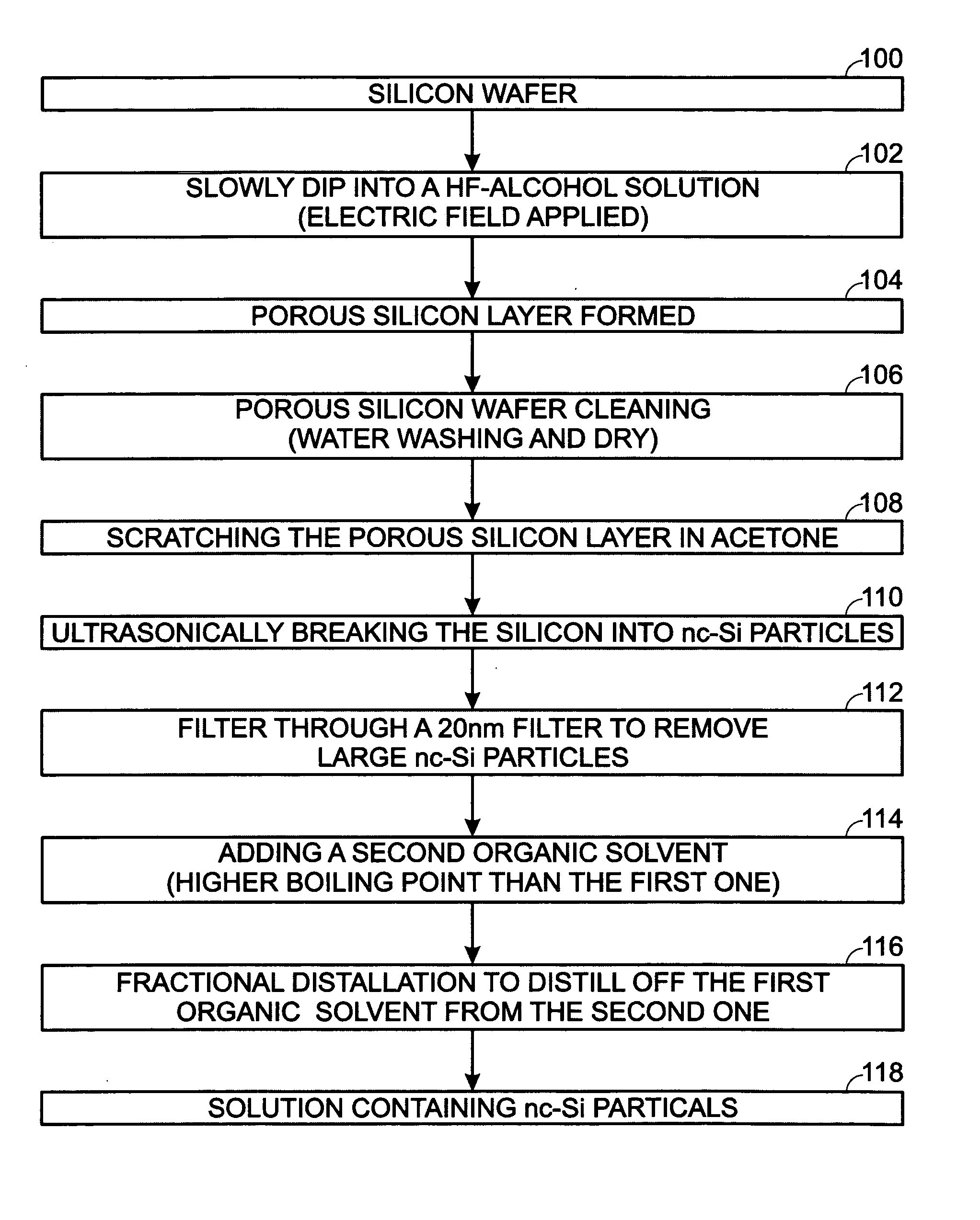
Figure 1 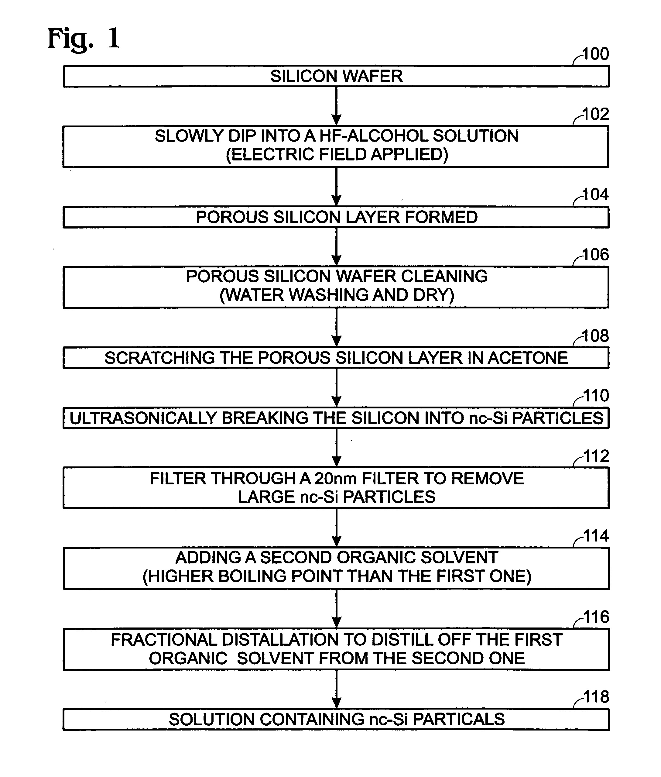
Figure 2 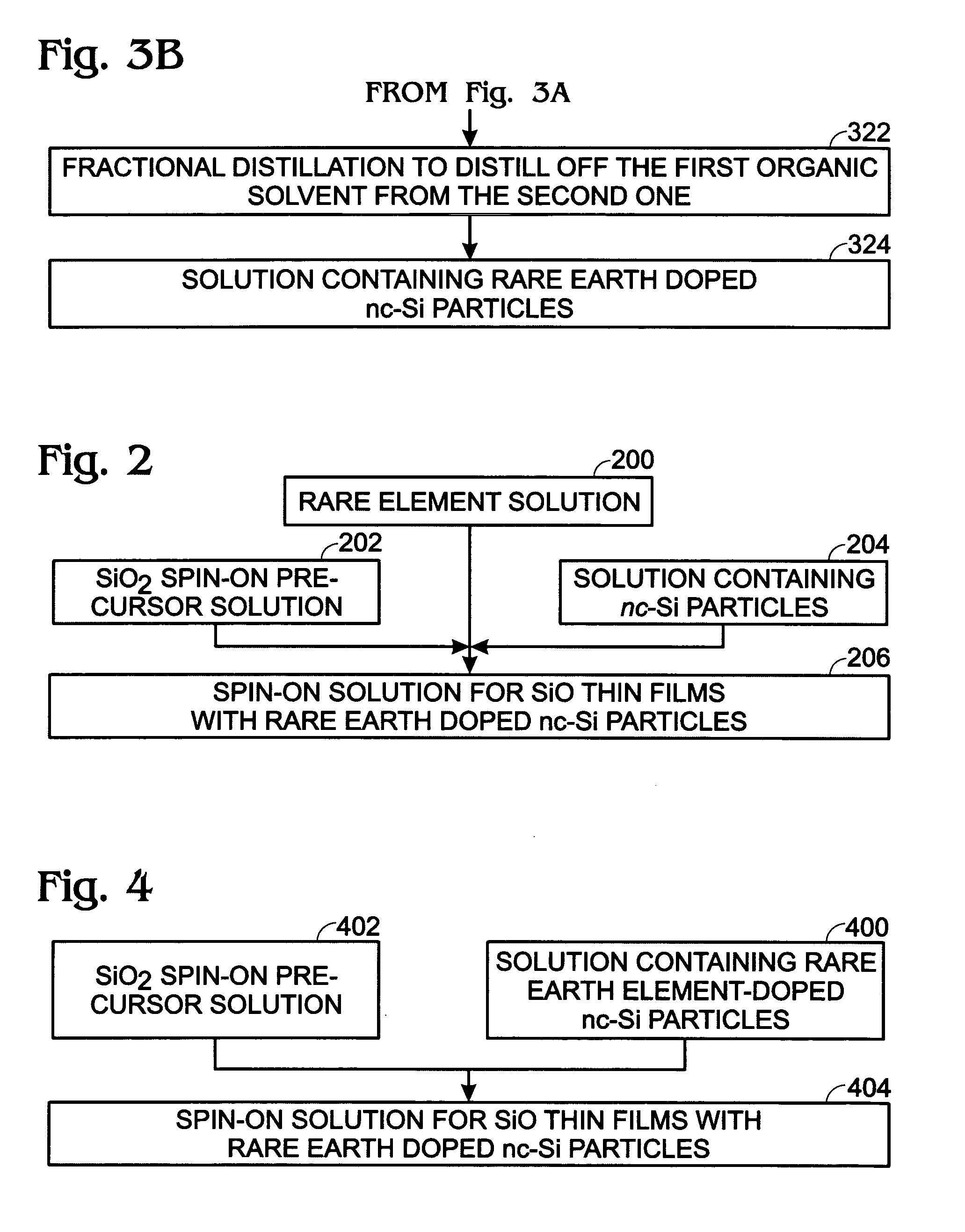
Figure 3
Abstract
Description
RELATED APPLICATIONS
[0001] The application is a continuation-in-part of a pending application entitled RARE EARTH ELEMENT-DOPED SILICON / SILICON DIOXIDE LATTICE STRUCTURE, invented by Li et al., Ser. No. 11 / 039,463, filed on Jan. 19, 2005, which is incorporated herein by reference.BACKGROUND OF THE INVENTION
[0002] 1. Field of the Invention
[0003] This invention generally relates to integrated circuit (IC) fabrication and, more particularly, to a procedure for making a rare earth element-doped silicon oxide (SiO2) precursor with nanocrystalline (nc) Si particles, for use in silicon-based electroluminescence (EL) devices.
[0004] 2. Description of the Related Art
[0005] The observation of visible luminescence at room temperature, emanating from porous silicon (Si), has spurred a tremendous amount of research into using nano-sized Si to develop a Si-based light source. One widely used method of fabricating nanocluster Si (nc-Si) is to precipitate the nc-Si out of SiOx (x<2), produci...
Examples
Embodiment Construction
[0022]FIG. 1 is a diagram depicting a process for forming a nc Si solution. The synthesis of nc Si particles includes four basic steps. In the first basic step (Steps 100-108), a porous silicon layer is formed through an electrochemical etch process. The solution for the electrochemical process is the mixture of HF( about 49%) and alcohol, such as the methanol or ethanol. The porous silicon layer is formed by slowly immersing the wafer into the solution while keeping an electrical bias on the wafer. The thickness of the resulting porous silicon layer depends on the immersion speed, current density, solution concentration, and wafer properties.
[0023] The second step (Step 110) is the transfer of the porous silicon layer into an organic solvent. An ultrasonic treatment can be used in the step to separate the porous silicon layer from the wafer. The solvents used in this step include a strong polar organic solvent, such as acetone or tetrahydrofuran.
[0024] After transfer, the nc Si p...