
Semiconductor device
a technology of semiconductors and semiconductors, applied in static indicating devices, instruments, non-linear optics, etc., can solve the problems of air bubbles generated by color filters and contamination of crystal layers, and achieve the effect of further reducing the thickness and weight of the whole liquid crystal display devi
Patent Information
- Authority / Receiving Office
- US · United States
- Patent Type
- Applications(United States)
- Current Assignee / Owner
- Publication Date
- 2007-12-06
Smart Images
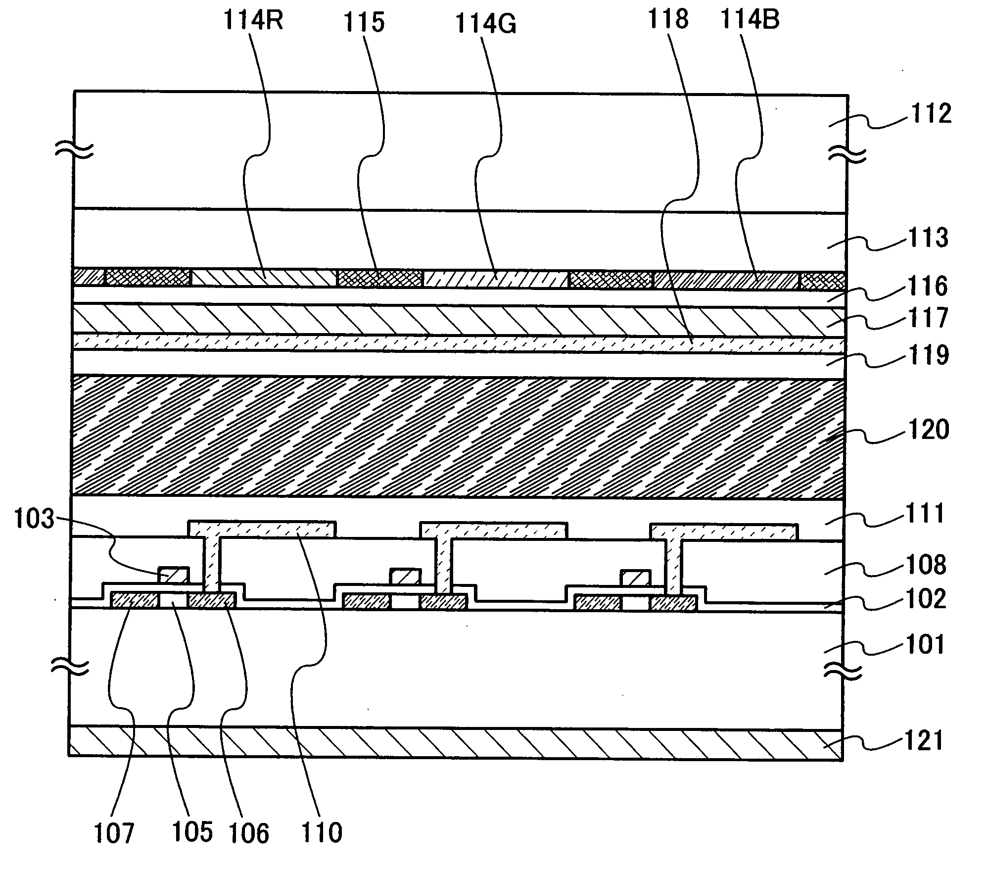
Figure 1 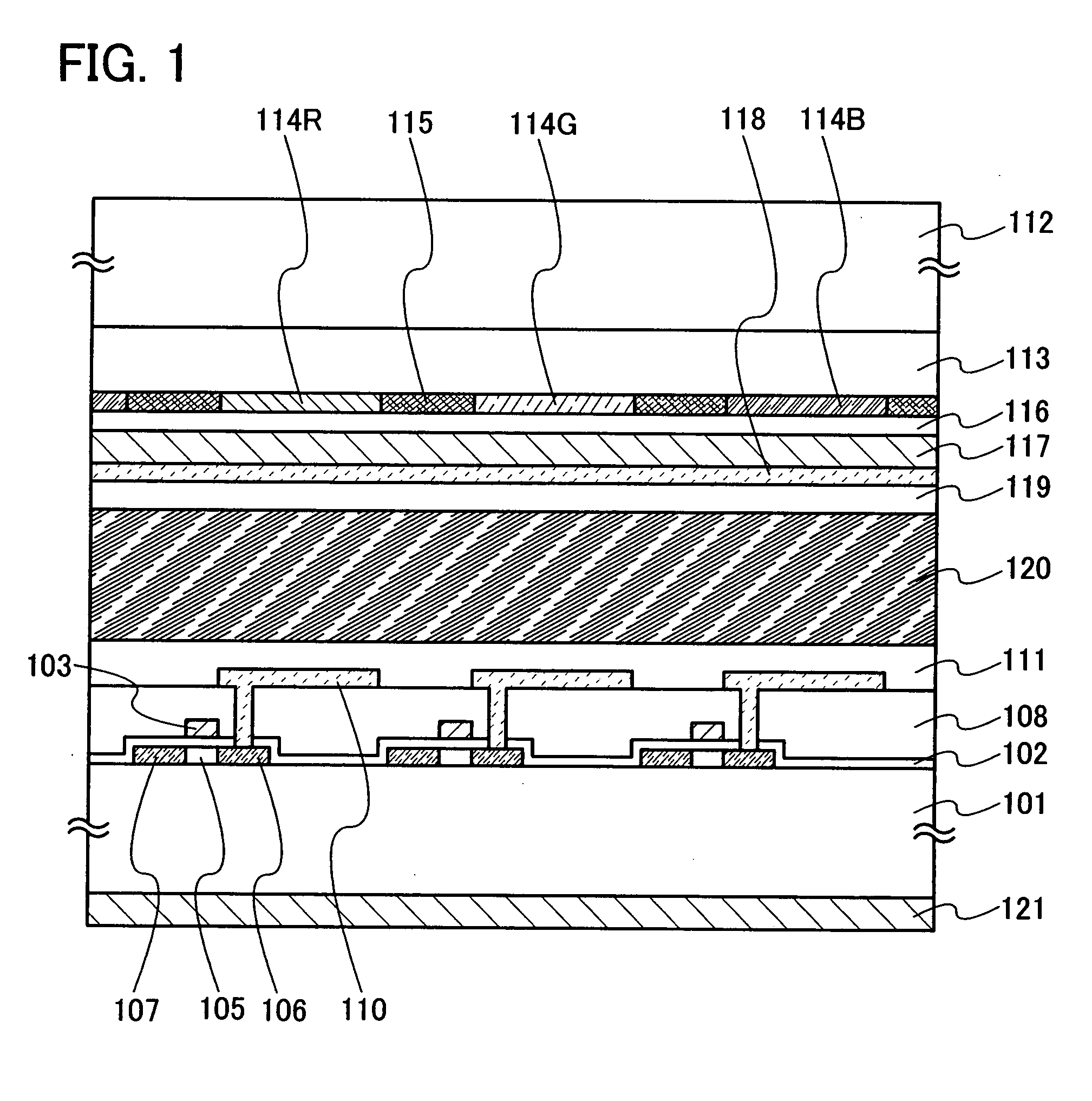
Figure 2 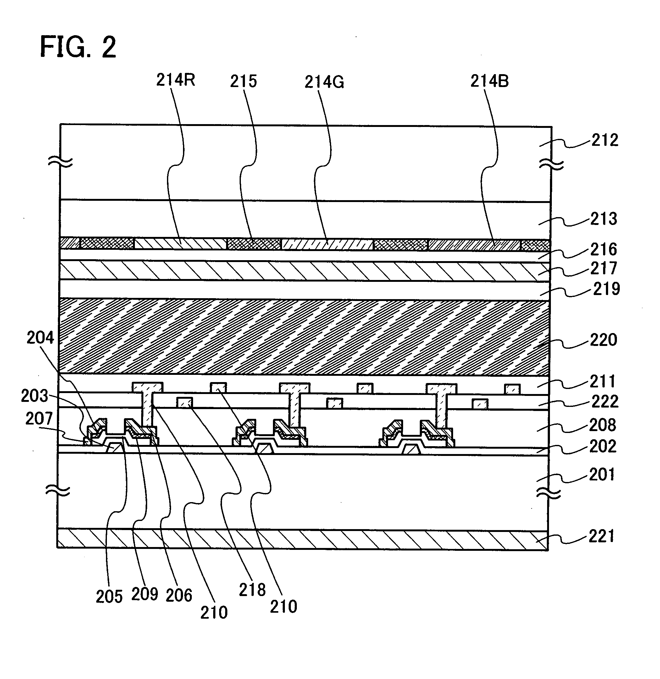
Figure 3
Abstract
Description
BACKGROUND OF THE INVENTION
[0001] 1. Field of the Invention
[0002] The present invention relates to a semiconductor device that has a circuit including a thin film transistor (hereinafter, referred to as a TFT) and a manufacturing method thereof. For example, the present invention relates to an electronic device on which an electro-optical device typified by a liquid crystal display panel is mounted as a component.
[0003] It is to be noted that the term “semiconductor device” in the present specification indicates a general device capable of functioning by utilization of semiconductor characteristics, and electro-optic devices, semiconductor circuits, and electronic devices are all included in the semiconductor device.
[0004] 2. Description of the Related Art
[0005] In recent years, a technique has attracted attention, in which a thin film transistor (TFT) is formed using a semiconductor thin film (a thickness of about several nm to several hundred nm) that is formed over a substrate having ...
Examples
embodiment mode 1
[0038]Here, an example of manufacturing a direct-view-type liquid crystal display device using TN (Twisted nematic) type liquid crystal with reference to FIG. 1.
[0039]First, a light interference layer 113 is formed over one surface of a first substrate 112 that is to be an opposite substrate. As the first substrate 112, a glass substrate is used.
[0040]The light interference layer 113 is provided to reduce reflection of external light at an interface that is formed from materials having different refractive indices. When the light interference layer 113 has a multilayer structure in which layers each having a different refractive index are stacked so that the interference layer 113 is widely effective to a wavelength region of visible light, external light reflected at interfaces of the stacked layers interferes and be canceled with each other; therefore, antireflection effect can be obtained. Here, the light interference layer 113 reduces reflection of external light at an interface...
embodiment mode 2
[0067]Although an example of the TN-type liquid crystal display device is shown in Embodiment Mode 1, in this embodiment mode, an example of an IPS (In Plane Switching) type liquid crystal display device is shown in FIG. 2. This IPS-type liquid crystal display device has a method in which a pixel electrode and a common electrode are formed over one of a pair of substrates that sandwich liquid crystal, and liquid crystal molecules are rotated in a plane between these electrodes, which is approximately parallel to a substrate surface, whereby switching of light is performed, and then display is performed. Since the liquid crystal molecules are rotated in an approximate parallel plane, inversions of gradation and hue are not generated due to a viewing angle, and accordingly, a wide viewing angle can be obtained as compared with the TN-type liquid crystal display device. In the IPS-type liquid crystal display device, arrangement of polarizing elements having dichroism is different from ...
embodiment 1
[0092]In this embodiment, an example in which the liquid crystal panel that is obtained in Embodiment Mode 1 or Embodiment Mode 2 is a liquid crystal module is shown in FIG. 3.
[0093]FIG. 3 is an explored perspective view of the liquid crystal module in which an LED (light emitting diode) is used as backlight. In a liquid crystal panel 302 obtained in Embodiment Mode 1 or Embodiment Mode 2, a plurality of driving ICs 305 are provided over an element substrate, and an FPC 307 that is electrically connected to a terminal provided over the element substrate is also provided.
[0094]A backlight 303 is arranged under the liquid crystal panel 302. In the backlight 303, a plurality of LEDs are used, and current is supplied from a connection code 306. As a light emitting material of the LED, an inorganic material or an organic material may be used.
[0095]It is to be noted that one kind of an LED that emits white light may be used, or three kinds of LEDs each of which emit red, blue, and green l...