
Manufacturing method package substrate
a manufacturing method and substrate technology, applied in the direction of printed element electric connection formation, conductive pattern formation, non-metallic protective coating application, etc., can solve the problems of difficult to realize fine pitches, circuit density drop, and missing bumps, so as to reduce the defect rate of bumps and uniform width and height
Patent Information
- Authority / Receiving Office
- US · United States
- Patent Type
- Applications(United States)
- Current Assignee / Owner
- Publication Date
- 2007-12-27
- Estimated Expiration
- Not applicable · inactive patent
Smart Images
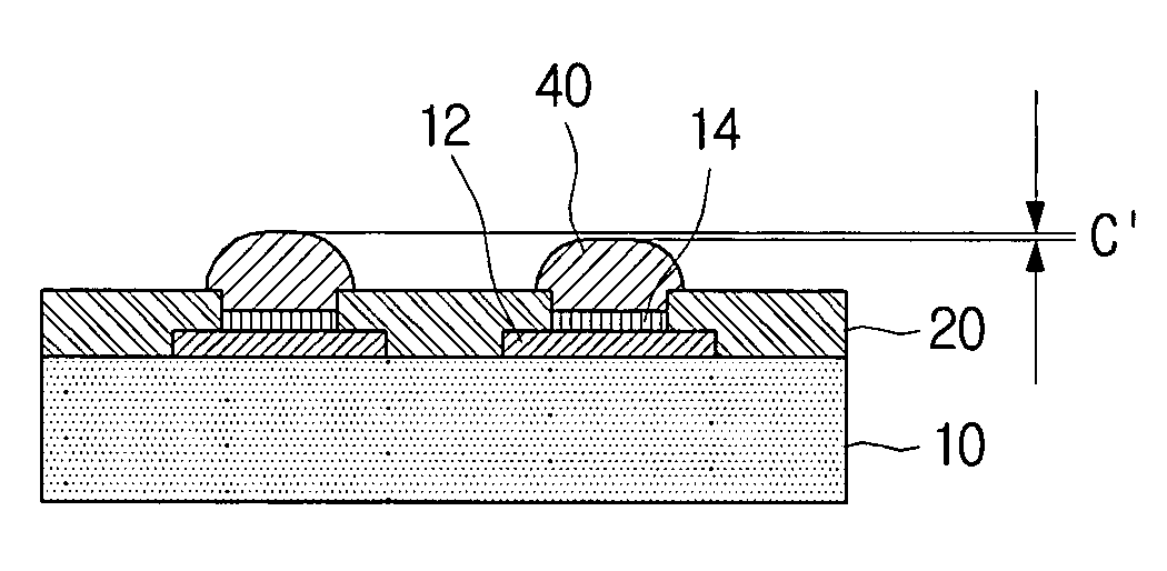
Figure 1 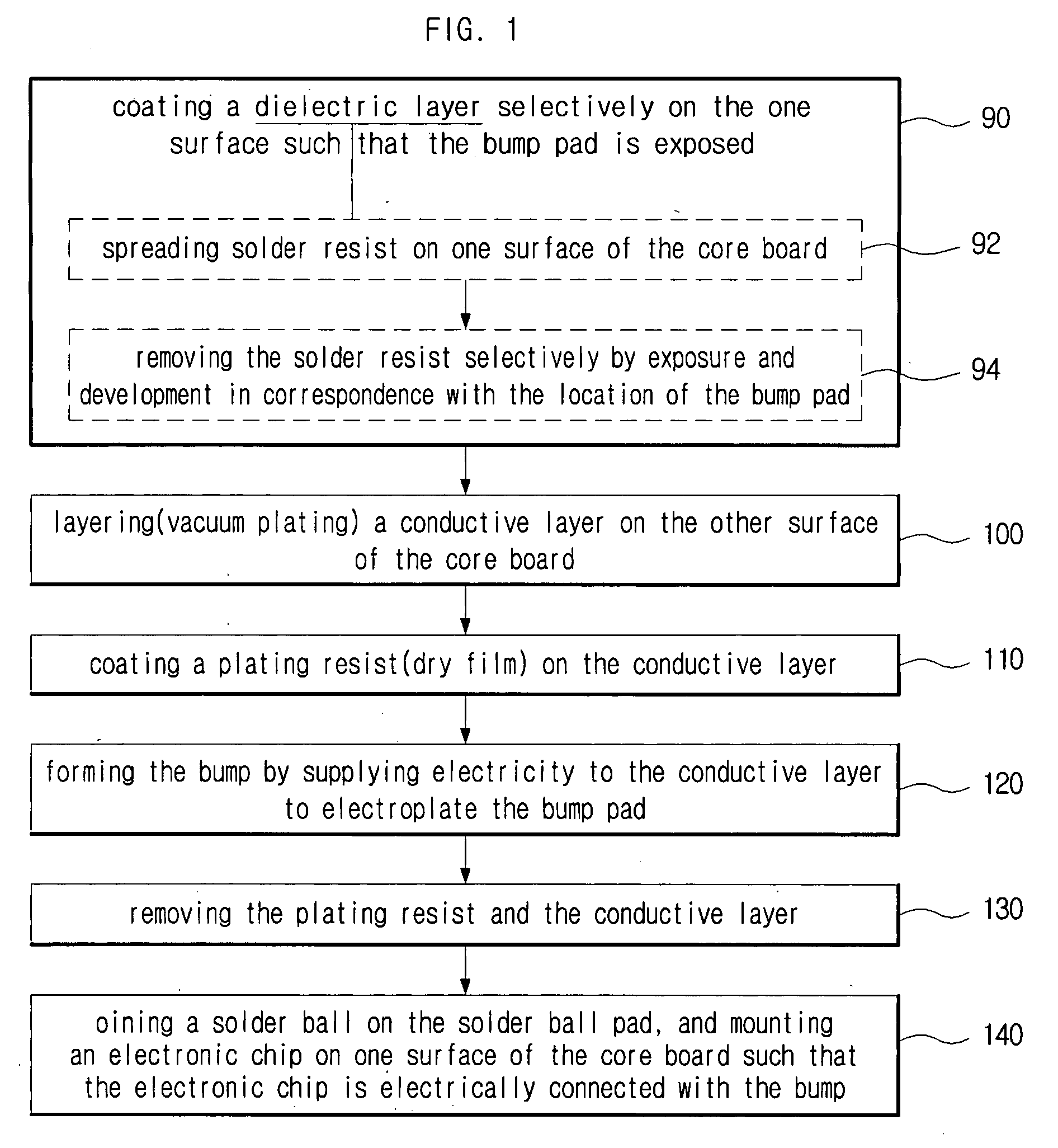
Figure 2 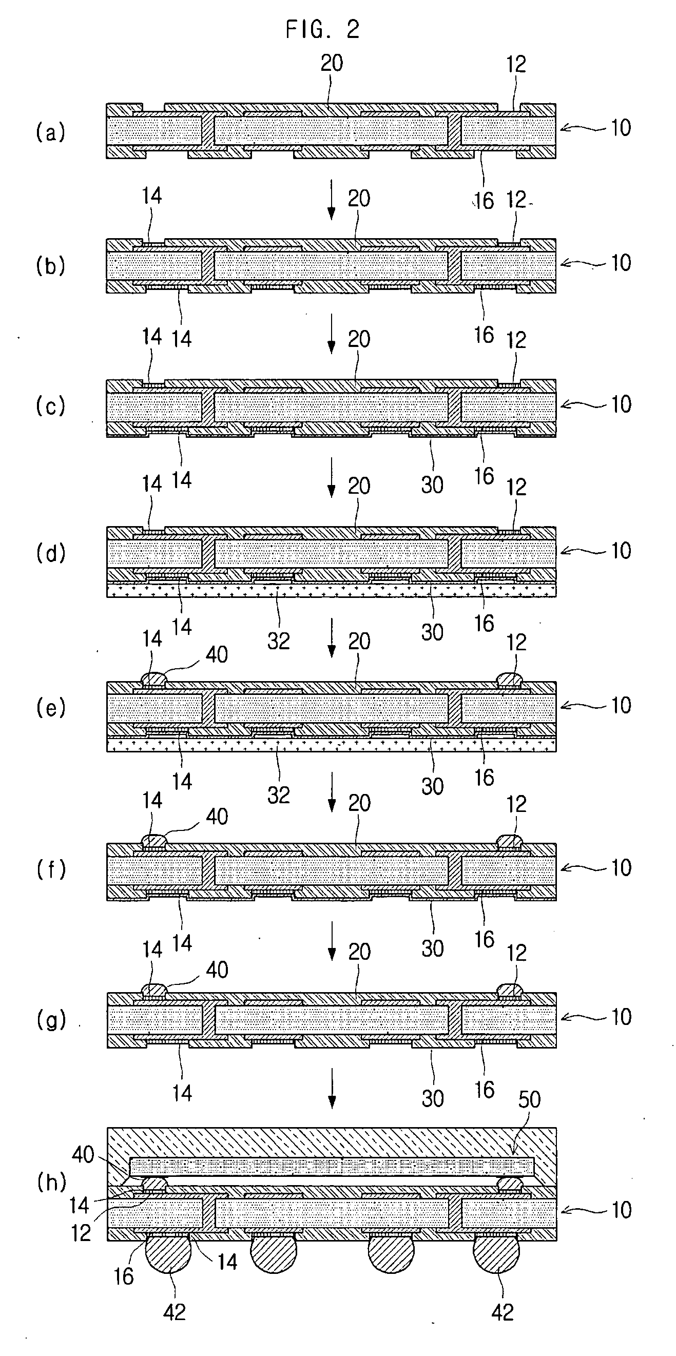
Figure 3
Abstract
Description
CROSS-REFERENCE TO RELATED APPLICATIONS
[0001] This application claims the benefit of Korean Patent Application No. 10-2006-0055833 filed with the Korean Intellectual Property Office on Jun. 21, 2006, the disclosure of which is incorporated herein by reference in its entirety.BACKGROUND
[0002] 1. Technical Field
[0003] The present invention relates to a manufacturing method of a package substrate.
[0004] 2. Description of the Related Art
[0005] A package substrate is a printed circuit board such as an FCP-(Flip chip package), CSP (Chip scale package), and BGA (Ball grid array) used in an electronic package where electronic chips are mounted, and the pitch, precision, reliability, and cost, etc., of electric contact points between a package substrate and an electronic chip mounted on its surface are very important factors which determine the performance of the package.
[0006] In the manufacturing process of a package substrate according to prior art, solder resist is first spread on the surface ...
Examples
Embodiment Construction
[0025]The manufacturing method of package substrate according to certain embodiments of the invention will be described below in more detail with reference to the accompanying drawings, in which those components are rendered the same reference number that are the same or are in correspondence, regardless of the figure number, and redundant explanations are omitted.
[0026]FIG. 1 is a flow chart illustrating a manufacturing method of a package substrate according to an embodiment of the present invention, FIG. 2 is a schematic diagram illustrating a manufacturing process of a package substrate according to an embodiment of the present invention, and FIG. 3 is a sectional view illustrating a package substrate according to an embodiment of the present invention. Referring to FIG. 2 and FIG. 3, a core board 10, bump pads 12, electroless plated layers 14, solder ball pads 16, solder masks 20, a conductive layer 30, a plating resist 32, bumps 40, solder balls 42, and an electronic chip 50 a...