
Method for forming a strained transistor by stress memorization based on a stressed implantation mask
a stress memorization and transistor technology, applied in the direction of transistors, semiconductor devices, electrical devices, etc., can solve the problems of reducing the controllability of the channel, reducing the size of the transistor, plurality of additional process steps, etc., to reduce the overall production cost of highly advanced integrated circuits, reduce the number of lithography steps, and reduce the overall production cost
Patent Information
- Authority / Receiving Office
- US · United States
- Patent Type
- Applications(United States)
- Current Assignee / Owner
- Publication Date
- 2008-01-31
Smart Images
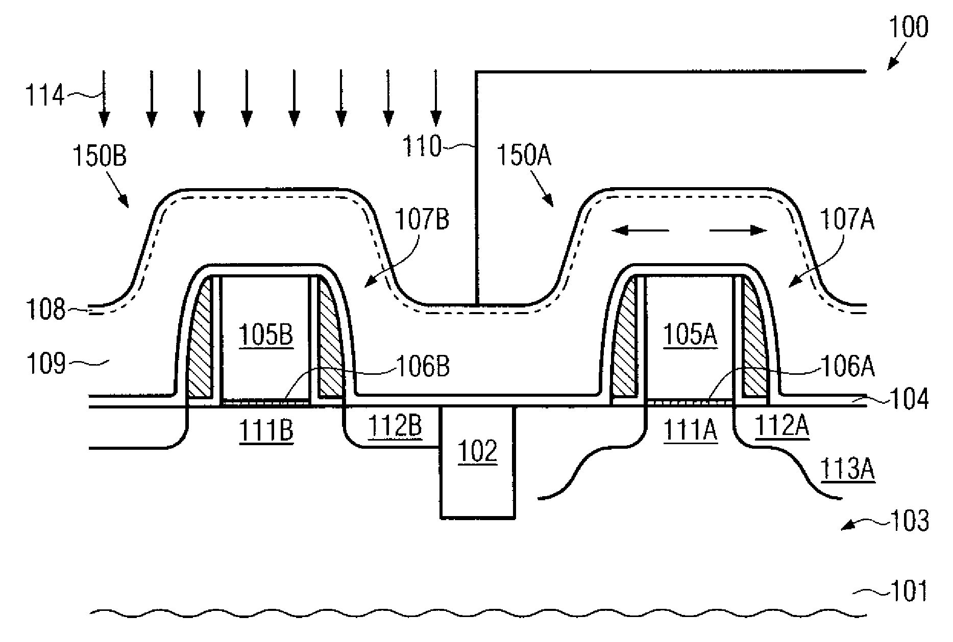
Figure 1 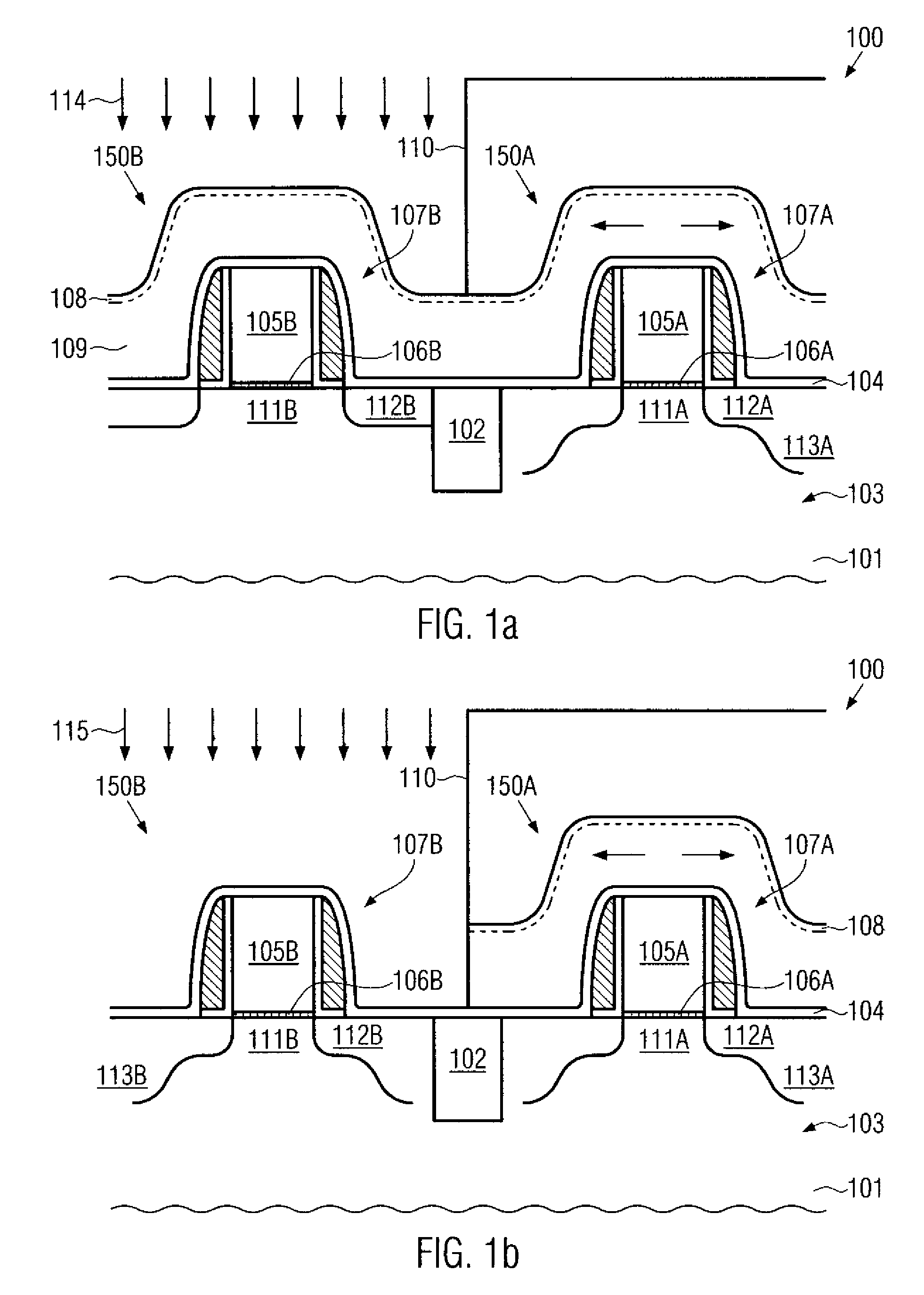
Figure 2 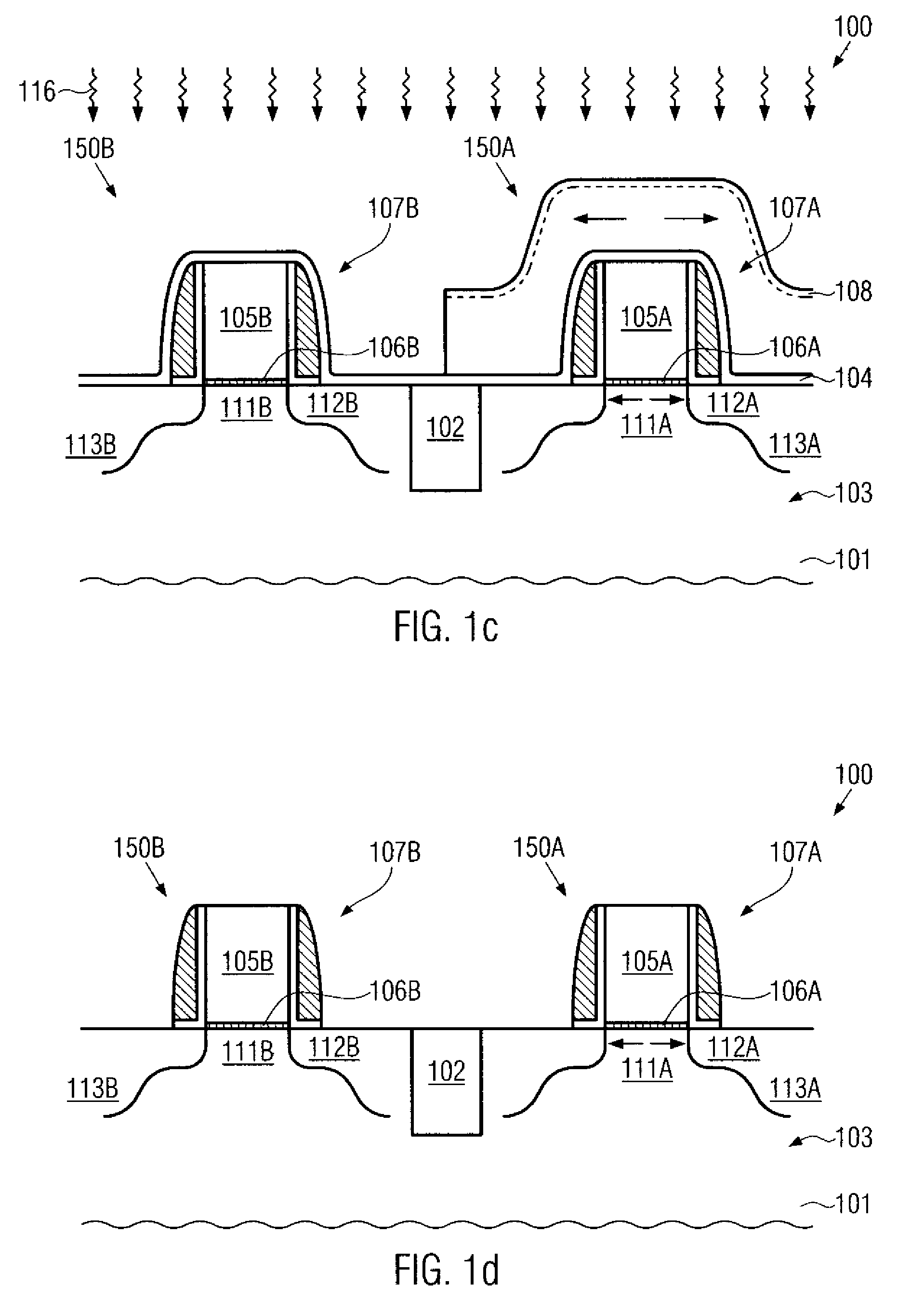
Figure 3
Abstract
Description
BACKGROUND OF THE INVENTION
[0001] 1. Field of the Invention
[0002] Generally, the subject matter disclosed herein relates to the formation of integrated circuits, and, more particularly, to the formation of transistors having strained channel regions by using stress-inducing sources, such as stressed overlayers and the like, so as to enhance charge carrier mobility in the channel region of an MOS transistor.
[0003] 2. Description of the Related Art
[0004] The fabrication of integrated circuits requires the formation of a large number of circuit elements on a given chip area according to a specified circuit layout, wherein a field effect transistor is an essential component in complex circuits comprising digital circuitry. Generally, a plurality of process technologies are currently practiced, wherein, for complex circuitry, such as microprocessors, storage chips and the like, CMOS technology is currently one of the most promising approaches due to the superior characteristics in view of op...
Examples
Embodiment Construction
[0022]Various illustrative embodiments of the invention are described below. In the interest of clarity, not all features of an actual implementation are described in this specification. It will of course be appreciated that in the development of any such actual embodiment, numerous implementation-specific decisions must be made to achieve the developers' specific goals, such as compliance with system-related and business-related constraints, which will vary from one implementation to another. Moreover, it will be appreciated that such a development effort might be complex and time-consuming, but would nevertheless be a routine undertaking for those of ordinary skill in the art having the benefit of this disclosure.
[0023]The present subject matter will now be described with reference to the attached figures. Various structures, systems and devices are schematically depicted in the drawings for purposes of explanation only and so as to not obscure the present disclosure with details ...