
Tunable voltage isolation ground to ground ESD clamp
a voltage isolation and ground technology, applied in semiconductor devices, semiconductor/solid-state device details, transistors, etc., can solve the problems of difficult coupling of power domains, prohibitive, and undesirable for most applications
Patent Information
- Authority / Receiving Office
- US · United States
- Current Assignee / Owner
- Publication Date
- 2009-04-09
- Estimated Expiration
- Not applicable · inactive patent
Smart Images
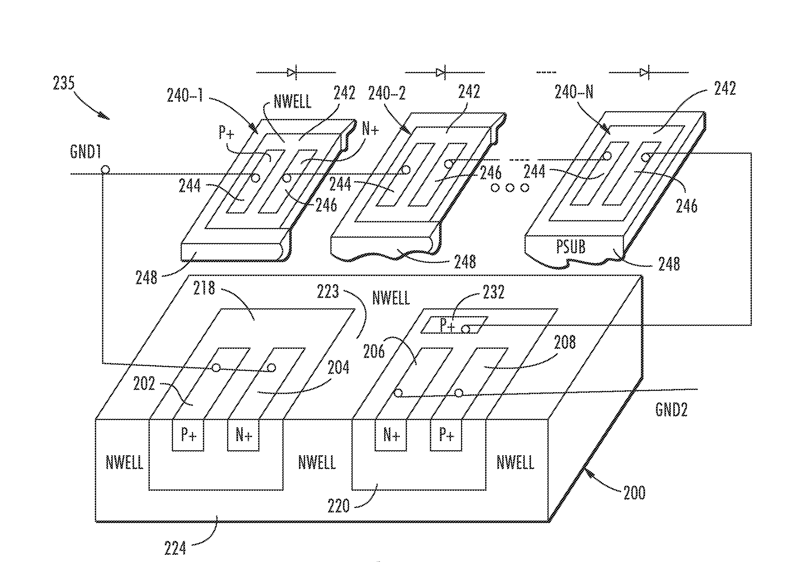
Figure 1 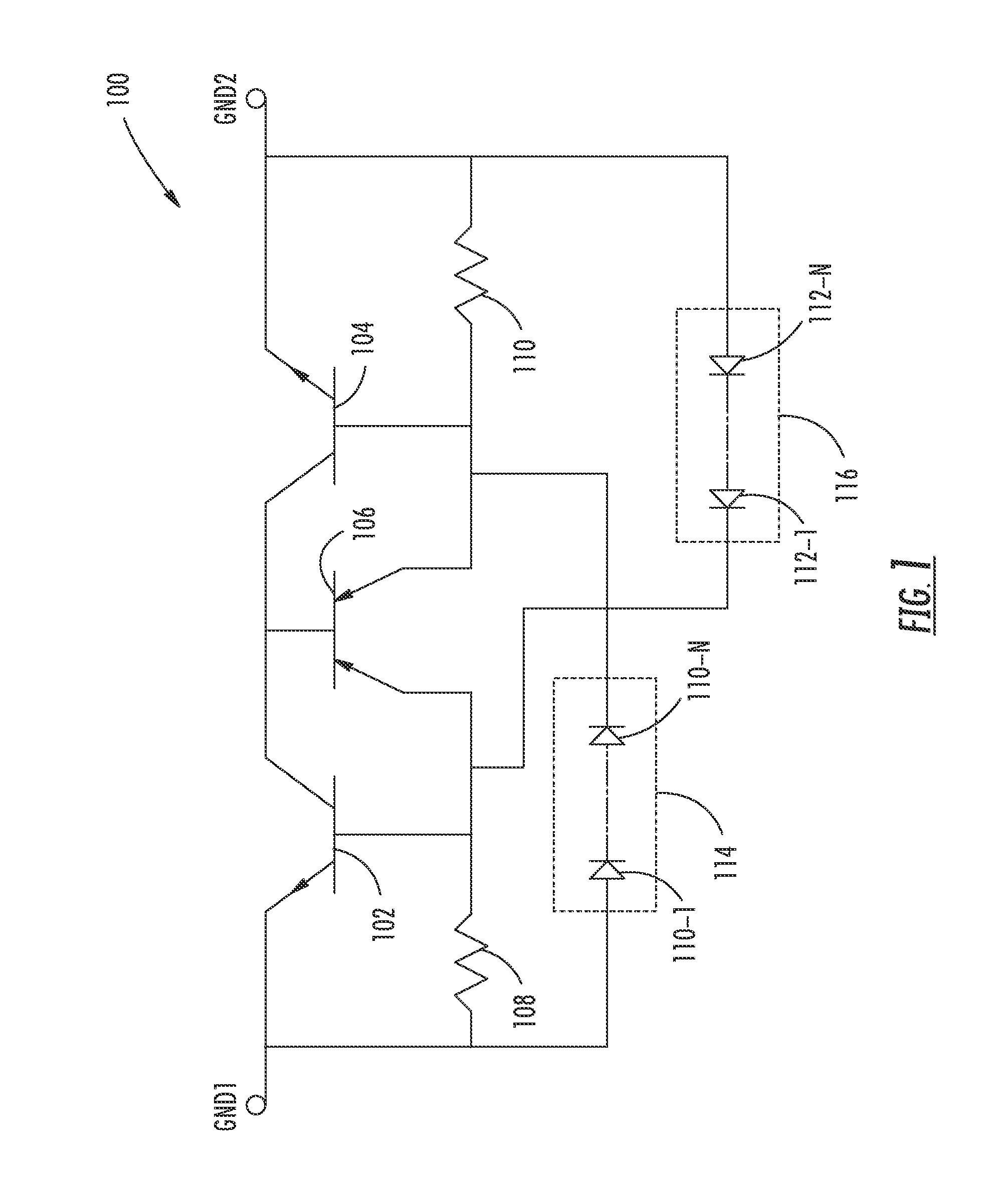
Figure 2 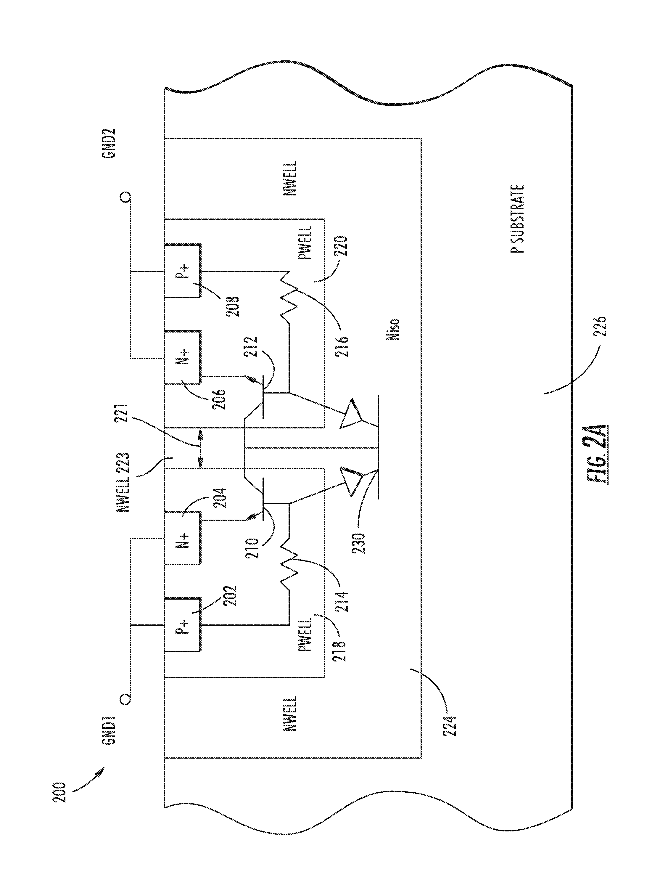
Figure 3
Abstract
Description
BACKGROUND
[0001] Power management parts typically have at least two power domains: Analog and Power. The analog domain is generally free of noise while the power domain, by definition, will have a lot of noise from the switching transistors (inductive transients).
[0002] Proper Electrostatic Discharge (ESD) protection for integrated circuits (IC's), such as power management parts, requires a defined current path between each pin combination. This requirement poses problems from a circuit design perspective when it is desired to keep the noisy switching power domain separate from the quiet analog domain. The supplies may be at different potentials (i.e. 5 V and 12 V) making coupling the power domains difficult.
[0003] The simplest solution, since both grounds are at zero volts, is to put anti-parallel diodes between the two grounds thereby tying the two domains together. This separates the grounds by a diode drop and the diode capacitance. Since transients, switching noise, on the power d...
Examples
Embodiment Construction
[0017]In the following detailed description, reference is made to the accompanying drawings, which form a part hereof, and in which is shown by way of illustration specific embodiments in which the inventions may be practiced. These embodiments are described in sufficient detail to enable those skilled in the art to practice the invention, and it is to be understood that other embodiments may be utilized and that logical, mechanical and electrical changes may be made without departing from the spirit and scope of the present invention. The following detailed description is, therefore, not to be taken in a limiting sense, and the scope of the present invention is defined only by the claims and equivalents thereof.
[0018]Embodiments of the present invention provide a single element between the grounds that provides both a high and adjustable isolation voltage during circuit operation and a low resistance / low voltage path under an ESD transient event. This is accomplished in embodiments...