
Nitride Semiconductor Light Emitting Device and Fabrication Method Thereof
a technology of nitride semiconductor and light emitting device, which is applied in the direction of semiconductor/solid-state device manufacturing, semiconductor devices, semiconductor devices, etc., can solve the problems of affecting the gan layer is grown in the trench, and the reliability of the light emitting device is affected, so as to improve the efficiency of optical extraction and operational reliability of the nitride semiconductor light emitting device, improve the luminous efficiency, and improve the utilization
Patent Information
- Authority / Receiving Office
- US · United States
- Patent Type
- Applications(United States)
- Current Assignee / Owner
- Publication Date
- 2009-07-02
- Estimated Expiration
- Not applicable · inactive patent
Smart Images
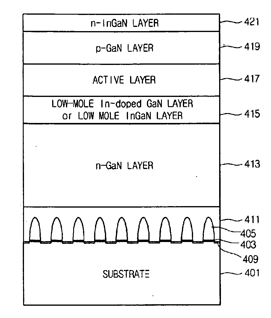
Figure 1 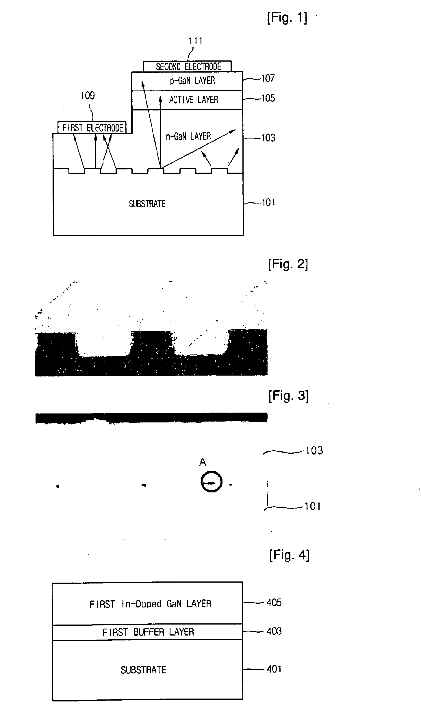
Figure 2 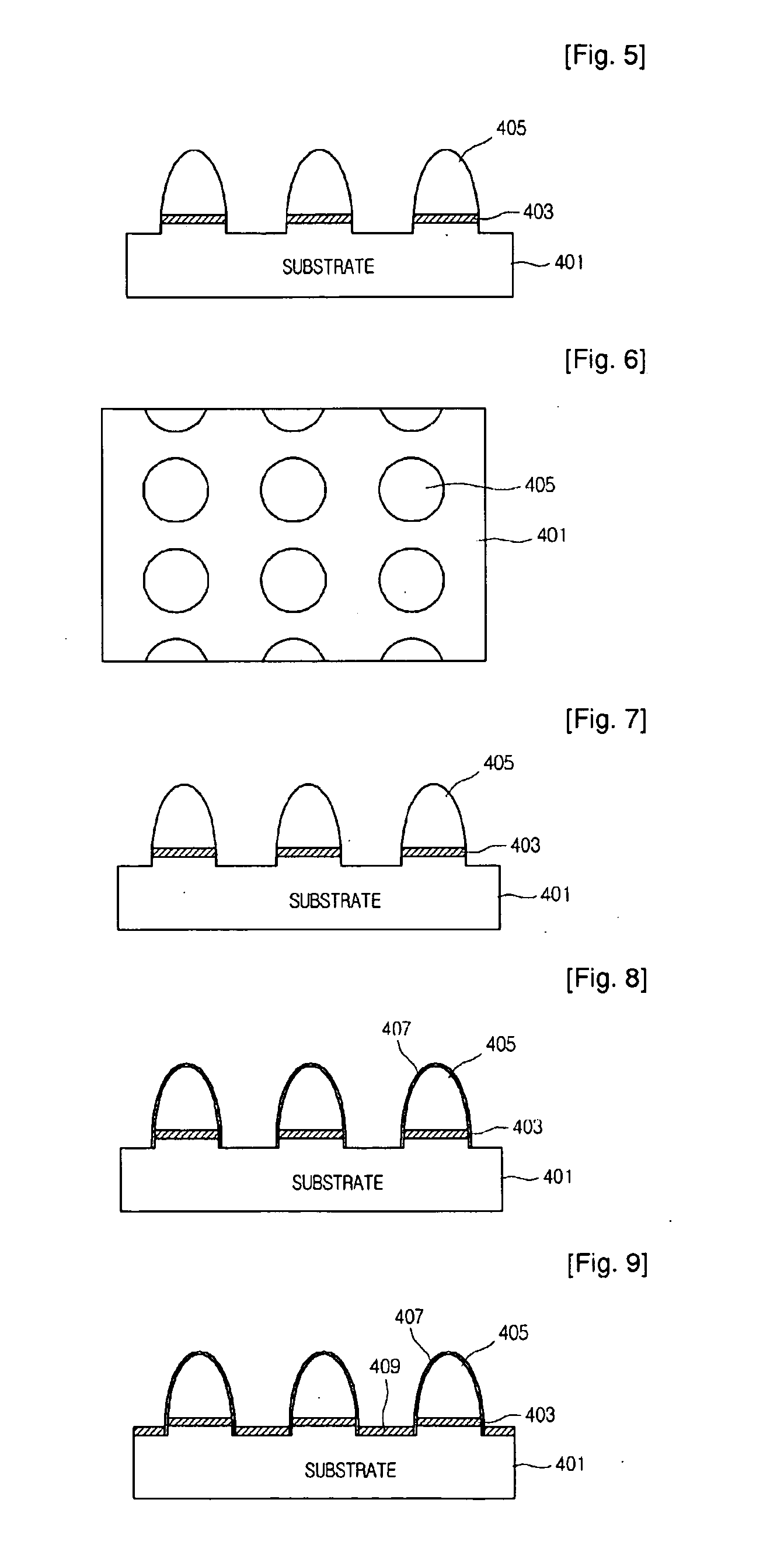
Figure 3
Abstract
Description
TECHNICAL FIELD
[0001] The present invention is relative to a nitride semiconductor light emitting device and fabrication method thereof, and to a nitride semiconductor light emitting device and a fabrication method thereof that can enhance the optical extraction efficiency.BACKGROUND ART
[0002] In order to increase the optical extraction efficiency of a nitride semiconductor light emitting device, a nitride semiconductor layer is grown on a patterned substrate.
[0003] In a related art method of fabricating a nitride semiconductor light emitting device, a sapphire substrate or a silicon carbide (SiC) substrate is selectively patterned in a predetermined shape by using a mask material. An exposed portion of the substrate is selectively dry etched. The mask material is then removed to thereby obtain a substrate with a predetermined pattern. A nitride semiconductor layer is grown on the patterned substrate.
[0004] FIG. 1 illustrates a stack structure of a related art nitride semiconductor ligh...
Examples
embodiment 1
[0033]FIGS. 4 to 6 are views illustrating a method of fabricating a selective etched GaN and sapphire substrate (SEGSS) structure in a nitride semiconductor light emitting device according to the present invention.
[0034]In order to fabricate an SEGSS substrate of the present invention, a first layer 403 and a first In-doped GaN layer 405 are sequentially formed on a substrate 401, resulting in a staked structure as illustrated in FIG. 4.
[0035]The substrate 401 may be a sapphire substrate, a silicon carbide substrate, a silicon substrate, or a GaAs substrate. The first buffer layer 403 may be a stack structure of AlInN / GaN, a supper lattice structure of InGaN / GaN, a stack structure of InxGa1−x N / GaN, or a stack structure of AlxInYGa1−(x+Y)N / InxGa1−xN / GaN. Although FIG. 4 illustrates an In-doped GaN layer 405 as the GaN layer formed on the first buffer layer 403, the GaN layer 405 can also be an undoped-GaN layer or a GaN layer formed by doping other material. For example, the doping ...
embodiment 2
[0064]FIGS. 11 and 12 are views illustrating a method of fabricating a nitride semiconductor light emitting device according to a second embodiment of the present invention. FIG. 13 is a sectional view of the nitride semiconductor light emitting device according to the second embodiment of the present invention.
[0065]Referring to FIGS. 11, 12 and 13, the second embodiment is similar to the first embodiment, except that the process of patterning the insulation layer 407 on the first In-doped GaN layer 405 is omitted. Therefore, the difference only will be described.
[0066]According to the second embodiment of the present invention, a secondary GaN layer is re-grown on the SEGSS structure, without performing the process of patterning the SiO2 insulation layer. The secondary GaN growth is performed in a state that the etched corn-shaped GaN layer and the surface of the etched sapphire substrate are exposed.
[0067]In the secondary re-growth of the GaN layer, due to the strain change cause...