
Characterizing performance of an electronic system
a technology of electronic systems and performance, applied in the field of electronic circuit simulation, can solve problems such as small penalties
Patent Information
- Authority / Receiving Office
- US · United States
- Current Assignee / Owner
- Publication Date
- 2009-11-19
- Estimated Expiration
- Not applicable · inactive patent
Smart Images
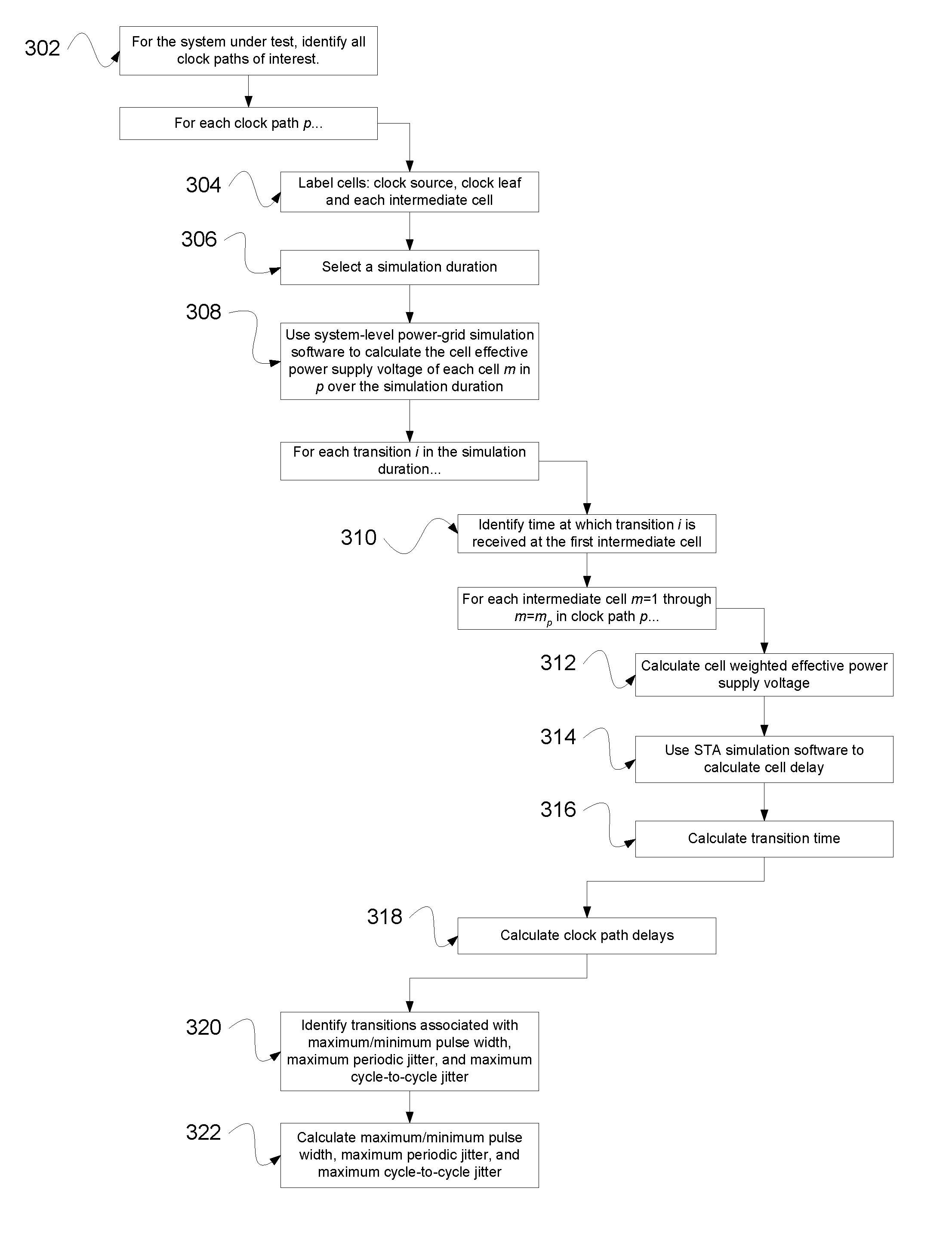
Figure 1 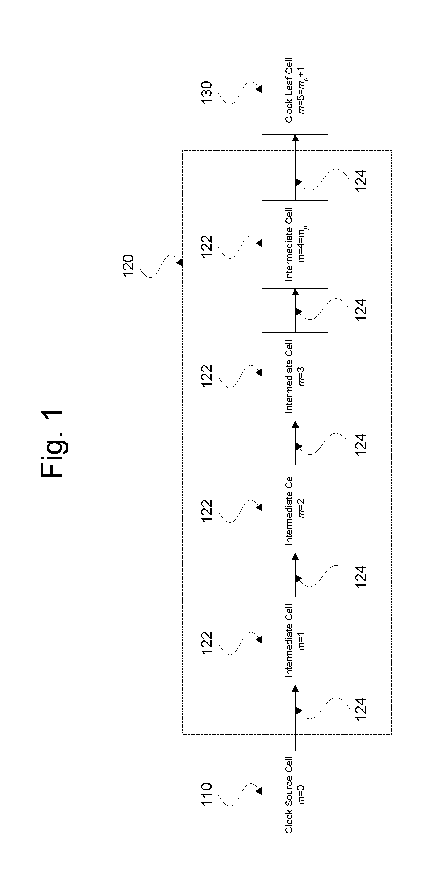
Figure 2 
Figure 3
Abstract
Description
BACKGROUND OF THE INVENTION
[0001] 1. Field of the Invention
[0002] The field of this invention is electronics, and particularly the simulation of electronic circuitry using computer-based simulation tools.
[0003] 2. Description of the Related Art
[0004] A typical integrated circuit (IC) contains thousands of clock paths. A clock path p is a sequence of one or more intermediate cells m that carry a clock signal from a clock source cell to a clock leaf cell. The number of intermediate cells in p is denoted mp. In a typical clock path, mp is 3-30. Each intermediate cell commonly contains 5-20 individual electronic components, e.g., transistors, diodes, etc.
[0005] FIG. 1 is a block diagram of a typical clock path 120. Clock path 120 connects clock source cell 110, e.g., a phase-locked loop, to clock leaf cell 130, e.g., a flip-flop. Clock source cell 110 is labeled m=0, and clock leaf cell 130 is labeled m=mp+1, in this case, 5. Clock path 120 comprises four intermediate cells 122, labeled m=1 ...
Examples
Embodiment Construction
[0034]FIG. 3 is an exemplary flowchart of steps to be performed in one embodiment of the present invention.
[0035]The first step (302) is to identify all clock paths of interest. Some clocks within a system may be slow enough that jitter is not a concern, and a designer can exclude those clocks' paths from the simulation.
[0036]In the second step (304), for each clock path of interest p, let mp equal the number of intermediate cells in clock path p. Label the clock source cell m=0. Label the intermediate cells m+1 . . . mp. Label the clock leaf cell m=mp+1. This numbering is illustrated in FIG. 1.
[0037]The third step (306) is to select a time duration for simulation, known as the simulation duration. Usually, the selected simulation duration is three to five times the duration of slowest significant cause of Veff,m variation. Typically, package inductance / board capacitance resonance (LC resonance) is the slowest significant cause of Veff,m variation. For example, if LC resonance of a ...