
Method for producing semiconductor wafer
a technology of semiconductor wafers and machining allowances, which is applied in the direction of manufacturing tools, cutting machines, edge grinding machines, etc., can solve the problems of increased machining allowance of silicon materials, and increased machining allowance of semiconductor materials, so as to reduce the kerf loss of semiconductor materials, reduce the machining allowance of semiconductor wafers, and obtain semiconductor wafers cheaply
Patent Information
- Authority / Receiving Office
- US · United States
- Patent Type
- Applications(United States)
- Current Assignee / Owner
- Publication Date
- 2009-12-17
- Estimated Expiration
- Not applicable · inactive patent
Smart Images
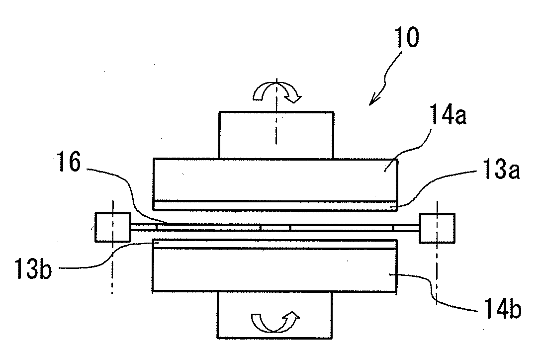
Figure 1 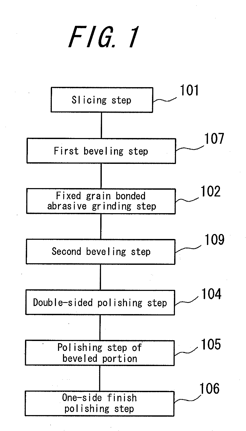
Figure 2 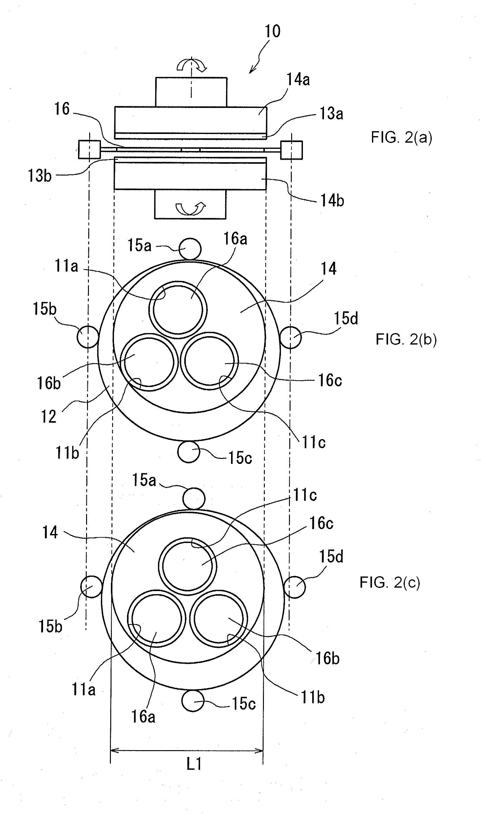
Figure 3
Abstract
Description
BACKGROUND OF THE INVENTION
[0001] 1. Field of the Invention
[0002] This invention relates to a method for producing a semiconductor wafer, and more particularly to a method for producing a semiconductor wafer by cutting out a thin disc-shaped semiconductor wafer from a crystalline ingot and then subjecting both surfaces thereof to a mirror finishing.
[0003] 2. Description of the Related Art
[0004] The conventional method for producing a semiconductor wafer typically comprises a series of a slicing step→a first beveling step→a lapping step→a second beveling step→a one-side grinding step→a double-sided polishing step→a one-side finish polishing step in this order.
[0005] In the slicing step, a thin disc-shaped semiconductor wafer is cut out from a crystalline ingot. In the first beveling step, an outer peripheral portion of the cut semiconductor wafer is beveled to suppress the occurrence of cracking or chipping in the semiconductor wafer at the subsequent lapping step. In the lapping step, th...
Examples
invention example 1
[0070]A silicon wafer having a diameter of 300 mm is prepared according to a flow chart shown in FIG. 1 according to the invention.
invention example 2
[0071]A silicon wafer having a diameter of 450 mm is prepared in the same production method as in Invention Example 1.
example 1
CONVENTIONAL EXAMPLE 1
[0072]A silicon wafer having a diameter of 300 mm is prepared by a production method shown in FIG. 4 inclusive of a lapping step.