
Semiconductor device
Patent Information
- Authority / Receiving Office
- US · United States
- Current Assignee / Owner
- Publication Date
- 2011-03-10
- Estimated Expiration
- Not applicable · inactive patent
Smart Images
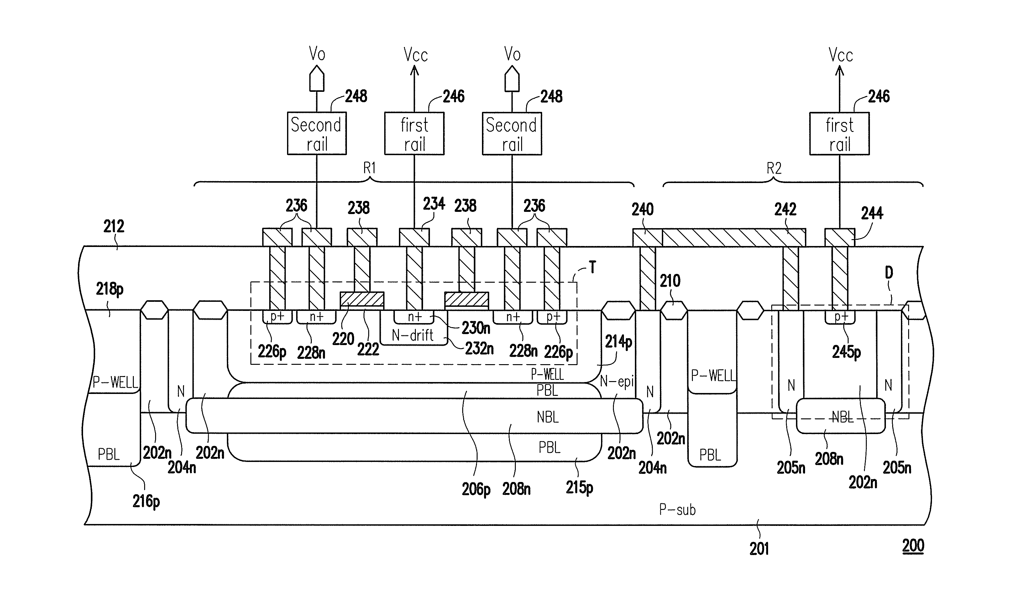
Figure 1 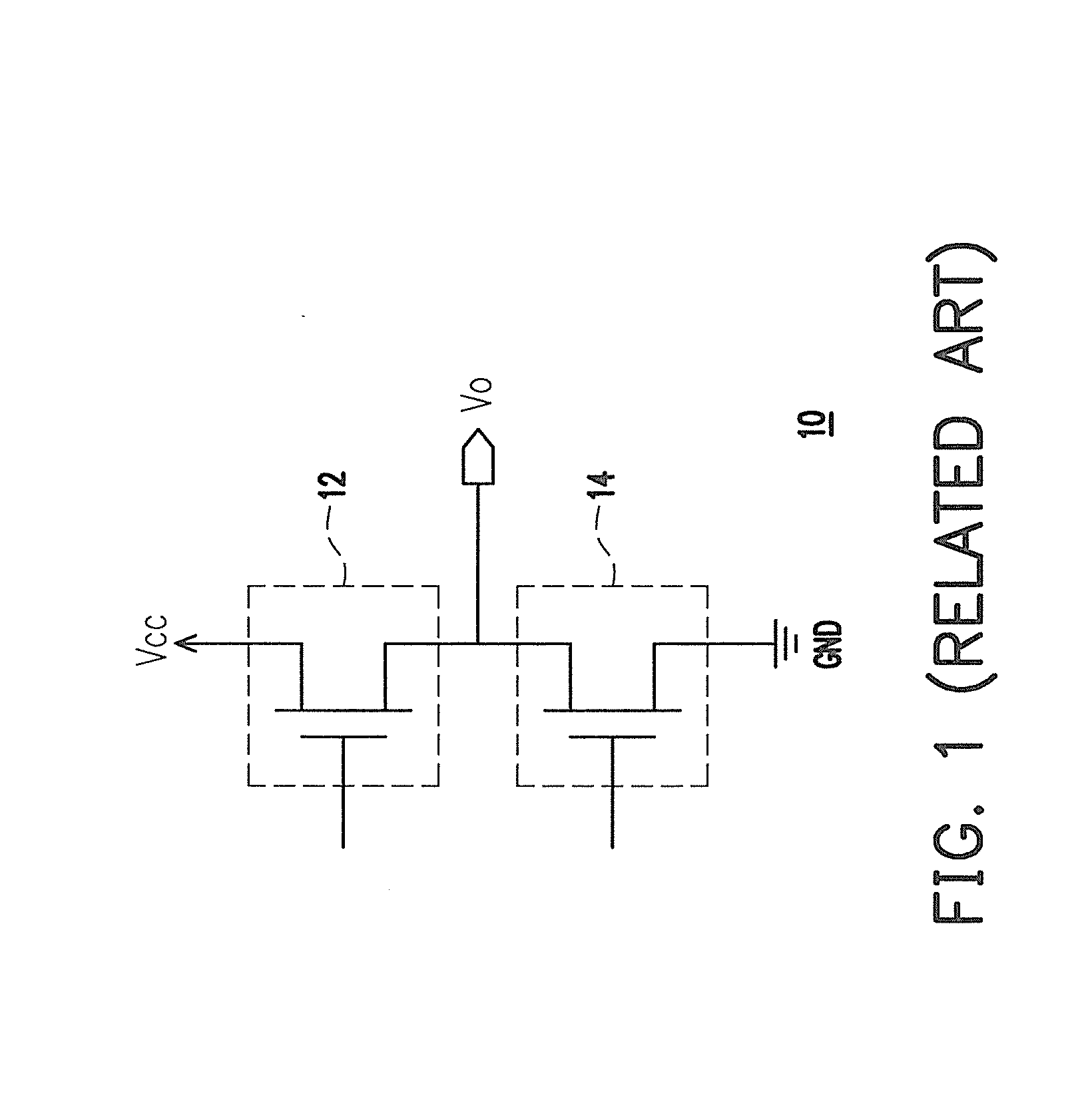
Figure 2 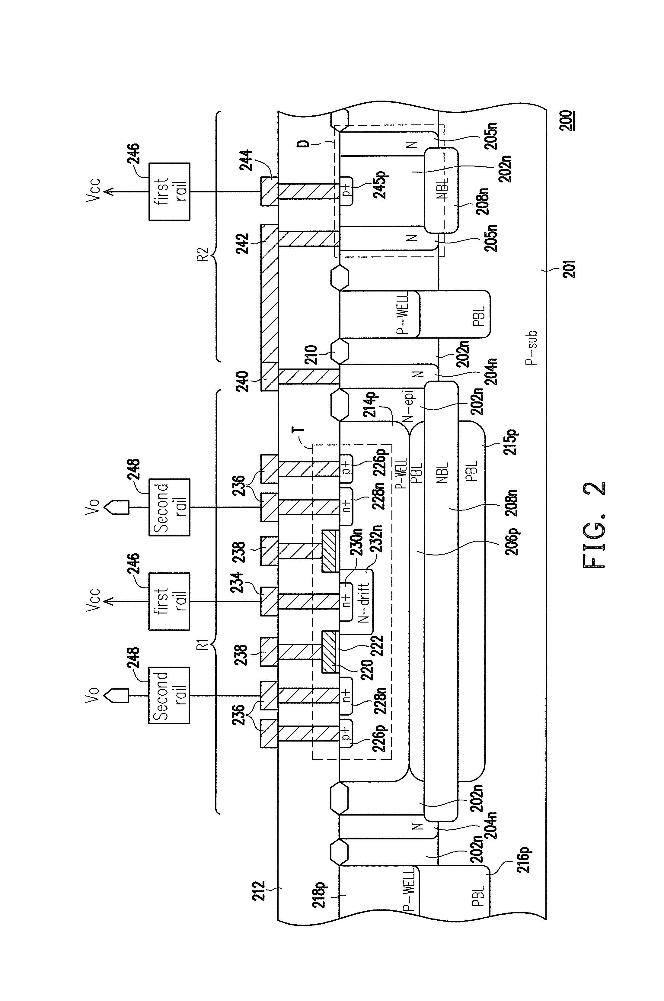
Figure 3
Abstract
Description
BACKGROUND OF THE INVENTION
[0001] 1. Field of the Invention
[0002] The invention generally relates to a semiconductor device, and more particularly, to a semiconductor device capable of being operated at a high voltage without a large substrate current.
[0003] 2. Description of Related Art
[0004] Semiconductor design has to be improved along with increasing integration and increasing complicated requirements thereof. For example, the design of high voltage devices must enable the high voltage devices to operate at a high voltage without effecting operation of other devices as well as large substrate currents.
[0005] FIG. 1 is a schematic view of a switch device formed by two high voltage n-type metal-oxide-semiconductors (HV-NMOS). Referring to FIG. 1A, the switch device 10 includes a high-side HV-NMOS 12 and a low-side HVNMOS 14, wherein a drain of the high-side HV-NMOS 12 is electrically connected to a system power Vcc, and a source of the high-side HV-NMOS 12 is electrically connected to ...
Examples
Embodiment Construction
[0017]FIG. 2 is a cross-sectional view of a semiconductor device according to an embodiment consistent with the invention. Referring to FIG. 2, in the invention, the semiconductor device 200 includes a substrate 201, an epitaxial layer 202n, a first sinker 204n, a transistor T, a diode unit D, a first buried layer 206p and a second buried layer 208n. Moreover, the semiconductor device 200 further includes an isolation structure 210, a dielectric layer 212, a well region 214p, a buried layer 216p, a well region 218p, interconnects 234, 236, 238, 240, 242, and 244, but the invention is not limited to the particular embodiment disclosed herein.
[0018]In the present embodiment, the transistor T, for example, is a high voltage n-type metal-oxide-semiconductor (HV-NMOS), wherein a drain 230n thereof is electrically connected to a first rail 246, and a source 228n thereof is electrically connected to a second rail 248. Accordingly, when the semiconductor device 200 is applied to a switch de...