
Glass substrate light emitting element and methods for manufacturing and luminescence thereof
a technology of light emitting elements and glass substrates, applied in the field ofluminescent materials, can solve the problems of low luminescent efficiency, restrict the application of field emissive devices, poor controllability and consistency, etc., and achieve the effects of improving the luminescent enhancing the spontaneous radiation and significantly increasing the internal quantum efficiency of the luminescent glass
Patent Information
- Authority / Receiving Office
- US · United States
- Patent Type
- Applications(United States)
- Current Assignee / Owner
- Publication Date
- 2012-12-27
- Estimated Expiration
- Not applicable · inactive patent
Smart Images
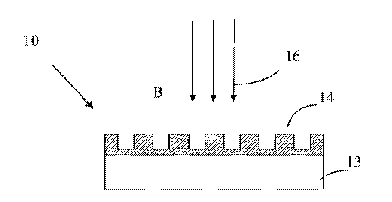
Figure 1 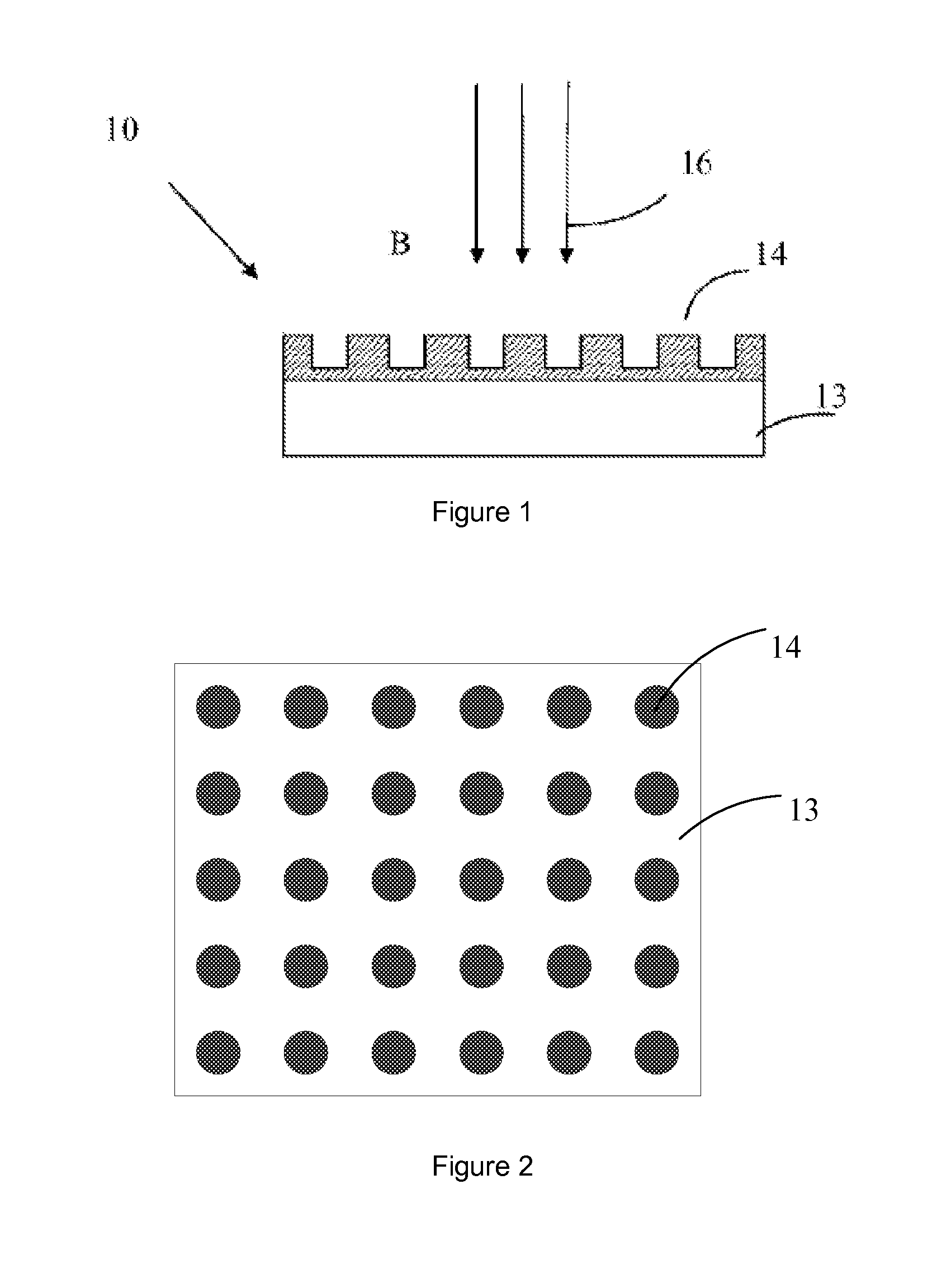
Figure 2 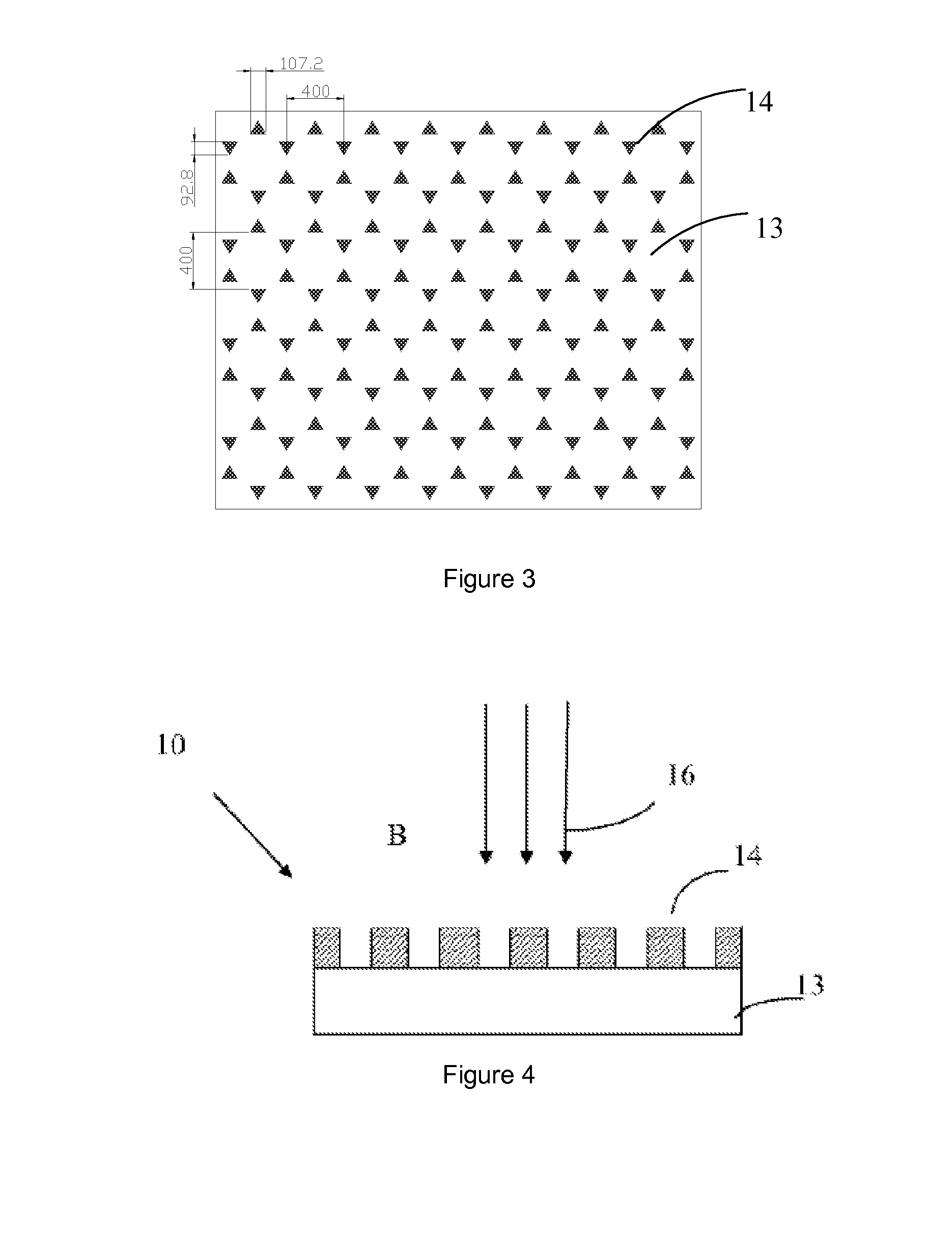
Figure 3
Abstract
Description
TECHNICAL FIELD
[0001] The present invention belongs to the technical field of luminescent materials, and specifically relates to a light emitting element having a glass substrate as a luminescent material, and methods for manufacturing and luminescence thereof.BACKGROUND ART
[0002] Conventional materials used for luminescent matrix include fluorescent powders, nano-crystals, glasses, and the like. Comparing with crystals and fluorescent powders, glasses have transparency, hardness, as well as good chemical stability and optical properties. In addition, glasses may be readily processed into products with various sizes and shapes, such as display devices or illuminating sources with various sizes and shapes.
[0003] For example, in the field of vacuum microelectronics, field emissive devices normally utilize a luminescent glass as the luminescent body, which shows broad application prospect in fields such as illumination and displays, and has drawn great attention from research entities fro...
Examples
example 1
[0050]The basic structure of the glass light emitting element of the present Example having a metal film is shown in FIG. 1. A green luminescent glass 13 having a size of 1×1 cm2 and surface-polished with 30Na2O.6Y2O3.60SiO2.4Tb2O3 (the numbers before the oxides represent molar ratio) is selected, and a metal layer 14 having an orderly periodic structure formed by the combination of six triangular pyramid-shaped sliver particles is formed on its surface with the currently used micro-processing technique. The structure scheme thereof is shown in FIG. 3. The specific structural parameters are also shown in FIG. 3. The height of the silver nano-particles is 30 nm. The luminescent glass 13 and the metal layer 14 constitute the light emitting element of the present Example.
[0051]The light emitting element manufactured in the present Example is bombarded with cathode rays produced by an electron gun. The electron beam passes through the metal layer 14 and then excites the luminescent glas...
example 2
[0053]The basic structure of the glass light emitting element of the present Example having a metal film is shown in FIG. 1. A green luminescent glass 13 surface-polished with 30Na2O.6Y2O3.60SiO2.4Tb2O3 (the numbers before the oxides represent molar ratio) is used, and an array of cylindrical sliver nano-particles arranged in a square lattice as shown in FIG. 4 is formed on its surface with the currently used micro-processing technique. These constitute the light emitting element of the present Example.
[0054]The periodic metal micro and nano structure make it possible to control the surface plasmon by constructing the surface configuration of the metal structure and by regulating the size parameters, and the enhancement to the luminescence is wavelength-selective. Taking the metal nano-array of the present Example as an example, assuming that the peak radiation wavelength of the luminescent glass 13 is λ, the dielectric constant of the metal layer 14 is εm, and the dielectric consta...
example 3
[0055]The basic structure of the glass light emitting element of the present Example having a metal film is shown in FIG. 1. A red luminescent glass 13 as prepared by the above method and surface-polished with 30Na2O.6Y2O3.60SiO2.4Eu2O3 (the numbers before the oxides represent molar ratio) is used, and an aluminum layer having a periodic micro and nano structure as shown in FIG. 1 is formed on its surface with the currently used micro-processing technique. The period of the structure is 700 nm. The size of the metal particles is 200 nm. The height of the metal layer 14 is 50 nm. The depth of the concaves to the surface of the metal layer 14 is 10 nm. These constitute the light emitting element of the present Example.