
Transfer substrate for forming metal wiring line and method for forming metal wiring line by means of said transfer substrate
a transfer substrate and metal wiring technology, applied in the direction of soldering equipment, manufacturing tools, liquid/solution decomposition chemical coating, etc., can solve the problem that the formation technique of metal plating cannot adequately deal with the miniaturization of metal, and achieve the effect of reducing load, stably transferring metal wiring, and suppressing damage to semiconductor chips or the like on the transfer targ
Patent Information
- Authority / Receiving Office
- US · United States
- Patent Type
- Applications(United States)
- Current Assignee / Owner
- Publication Date
- 2014-09-18
Smart Images
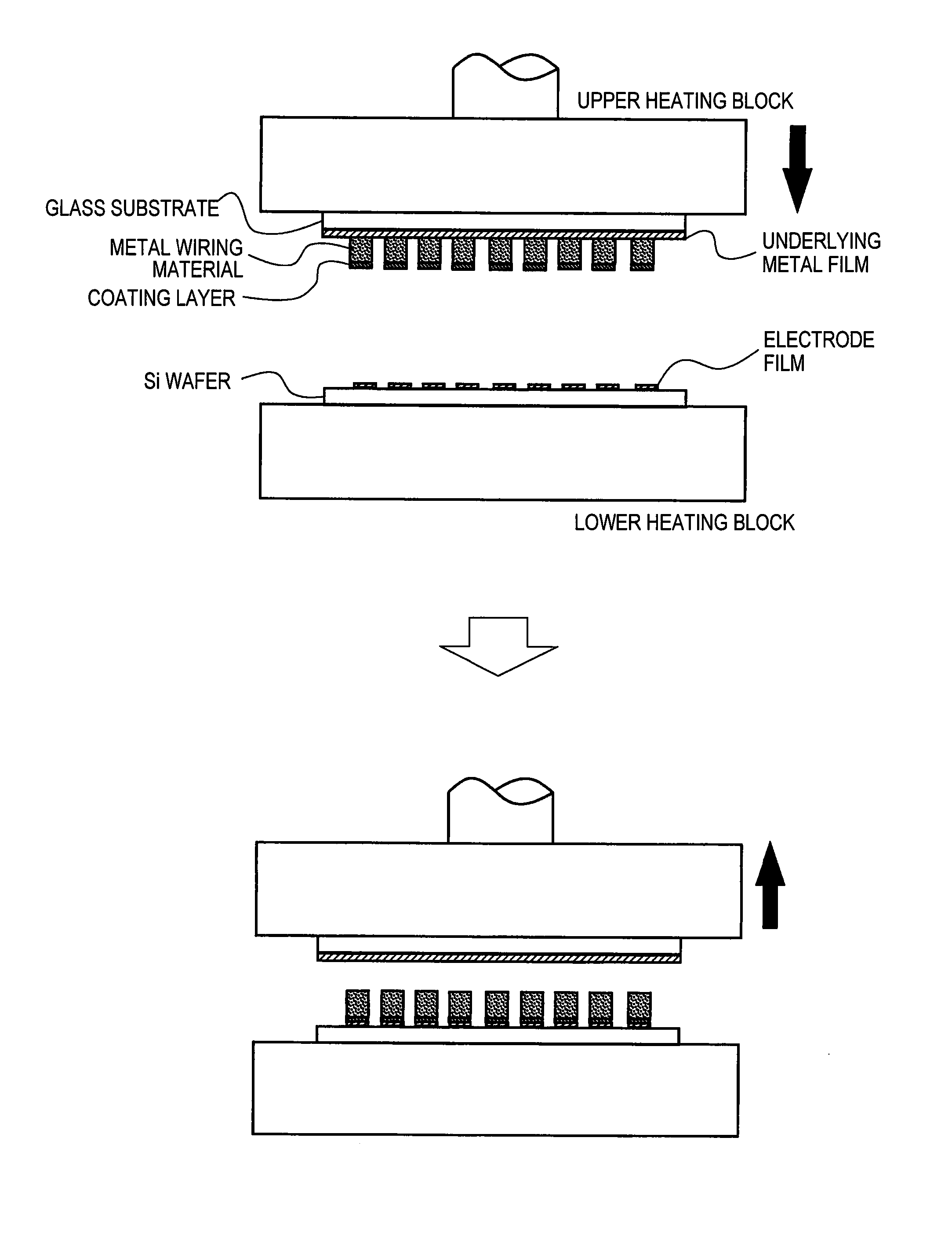
Figure 1 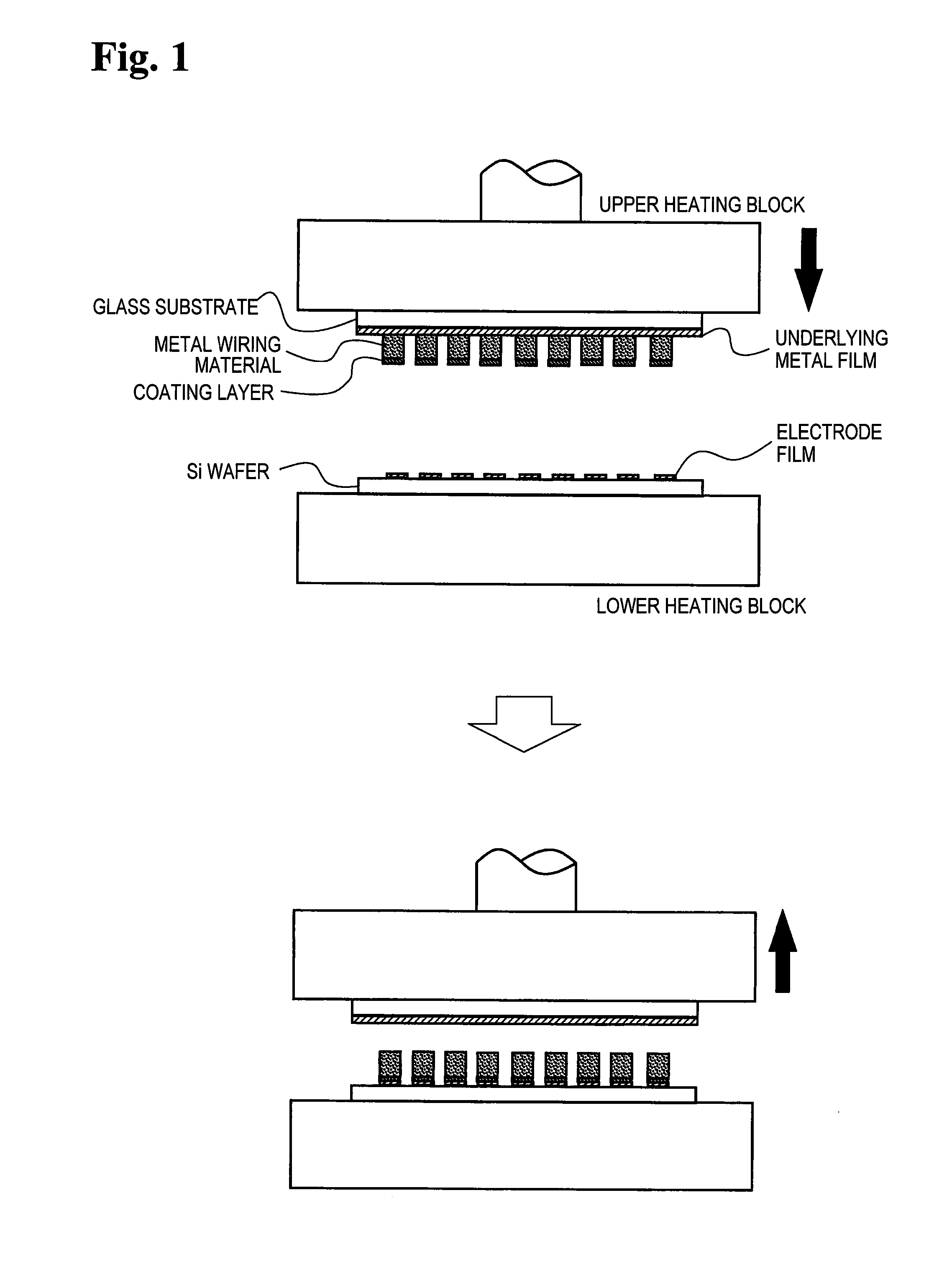
Figure 2
Abstract
Description
BACKGROUND OF THE INVENTION
[0001] 1. Field of the Invention
[0002] The present invention relates to a transfer substrate for forming a metal wiring on a transfer target such as a semiconductor wafer, a compound wafer and a MEMS wafer, and relates to a metal wiring method using the same.
[0003] 2. Description of the Related Art
[0004] With increasing packaging density of electronic components such as a semiconductor chip, their implementation method has changed from a conventional wire bonding method to a wireless implementation method such as a flip-chip bonding method in which a semiconductor chip is directly mounted on a circuit board, which has become a mainstream. A manufacturing process of electronic components using this implementation method is a process in which a bump is formed on a terminal electrode on a semiconductor chip of a device wafer or on an external electrode for connecting to a semiconductor chip, thus metal wiring being made up, and then this is face-down bonded onto ...
Examples
Embodiment Construction
[0039]First Embodiment: a transfer substrate was prepared with a glass substrate, and with this being used, metal wiring formation on a Si wafer was performed.
(Production of the Transfer Substrate)
[0040]First, Pt was film-formed with sputtering as an underlying metal film on a glass substrate (diameter size 100 mm, 4 inches, average thickness 500 μm). In the Pt film formation, after the glass substrate was subject to cleaning with reverse sputtering (Ar pressure 2.8×10⁻¹ Pa, RF output 250 W, sputtering time 60 seconds), the film formation was performed with use of a Pt target under conditions of Ar pressure 7.0×10⁻¹ Pa, DC output 500 W and sputtering time 115 seconds, and thus a Pt film having a thickness of 20 nm was formed.
[0041]Next, a metal wiring material was formed on a glass substrate with use of a metal paste made of Au powder. The metal paste used here was adjusted with a mixture of gold powder (average particle size: 0.3 μm) of a purity of 99.95 wt % produced with a wet re...