
Inter-Chip Alignment
a technology of inter-chips and waveguides, applied in the field of microchips, can solve the problems of inability to create various components of a sensing system from the same material, inability to cost-effectively integrate a waveguide and a detector on it, and inability to optimize the quality of detectors, etc., to achieve the effect of reducing the inter-chip spacing, reducing the coupling loss of waveguide and waveguide, and improving the coupling loss
Patent Information
- Authority / Receiving Office
- US · United States
- Patent Type
- Applications(United States)
- Current Assignee / Owner
- Publication Date
- 2017-06-22
Smart Images
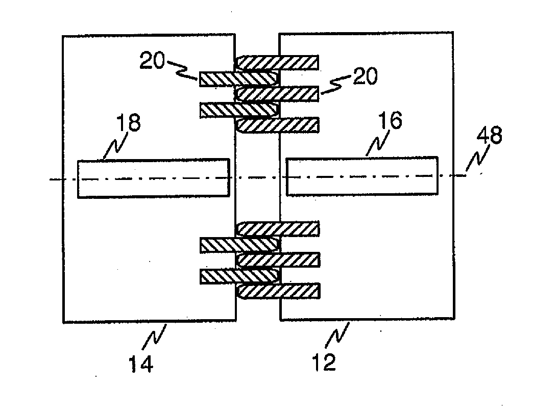
Figure 1 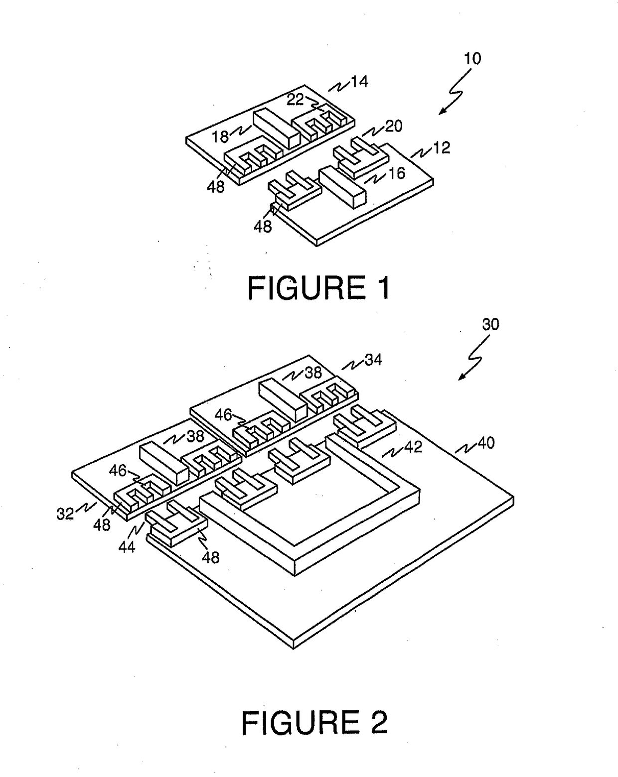
Figure 2 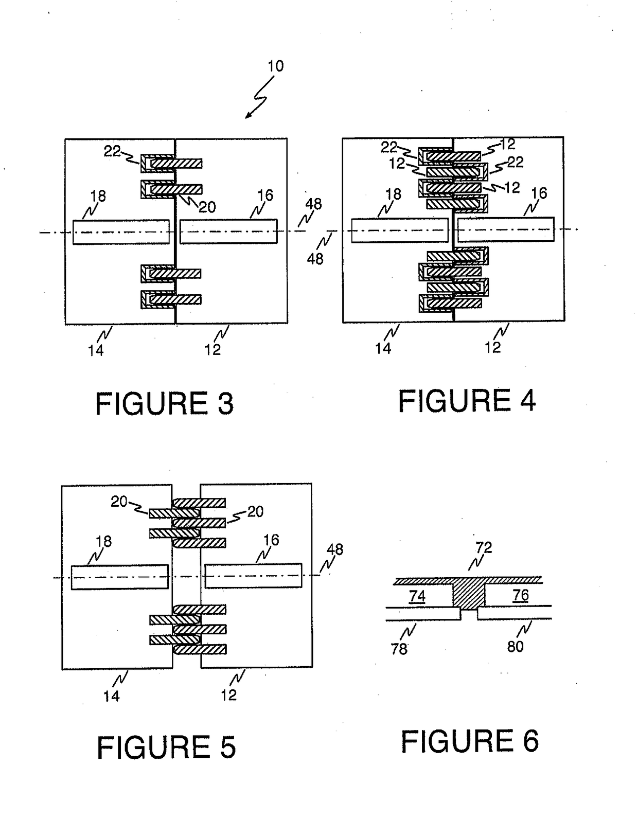
Figure 3
Abstract
Description
CROSS REFERENCE TO RELATED APPLICATIONS
[0001] This application is a continuation of U.S. patent application Ser. No. 14 / 158,079, filed Jan. 17, 2014 which claims the benefit of U.S. Provisional Patent Application No. 61 / 849,090, filed Jan. 18, 2013, both of which are incorporated herein by reference in their entirety.BACKGROUND OF THE INVENTION
[0002] Field of the Invention
[0003] The present invention relates generally to microchips and systems and devices employing microchips.
[0004] Description of Related Art
[0005] Quilt packaging is a new paradigm for inter-chip electrical communication. In quilt packaging conducting nodules that protrude from the vertical facets of integrated circuits are used for a dense, enhanced speed, and reduced-power interface between multiple dies within a package. See, e.g., G. H. Bernstein, Q. Liu, Z. Sun, and P. Fay, Quilt-packaging: a new paradigm for inter-chip communication; Proc. IEEE 7th Electronics Packaging Technology Conference, 2005, pp. 1-6; U.S. Pa...
Examples
Embodiment Construction
[0023]Persons of ordinary skill in the art will realize that the following description of the present invention is illustrative only and not in any way limiting. Other embodiments of the invention will readily suggest themselves to such skilled persons.
[0024]Referring first to FIG. 1, an isometric drawing shows how two optical components on two different integrated circuit chips can be optically coupled to one another using the teachings of the present invention. An assembly 10 is formed from a first integrated circuit chip 12 and a second integrated circuit chip 14. First integrated circuit chip 12 includes a first optical component 16 disposed on it. Optical component 16 may be an emitter, such as an integrated circuit laser, a detector, or a waveguide. Similarly, second integrated circuit chip 14 includes a second optical component 18 disposed on it. Optical component 18 may be an emitter, such as an integrated circuit laser, a detector, or a waveguide.
[0025]Integrated circuit ch...