
Apparatus and methods for predicting wafer-level defect printability
Patent Information
- Authority / Receiving Office
- US · United States
- Current Assignee / Owner
- Publication Date
- 2017-10-26
Smart Images
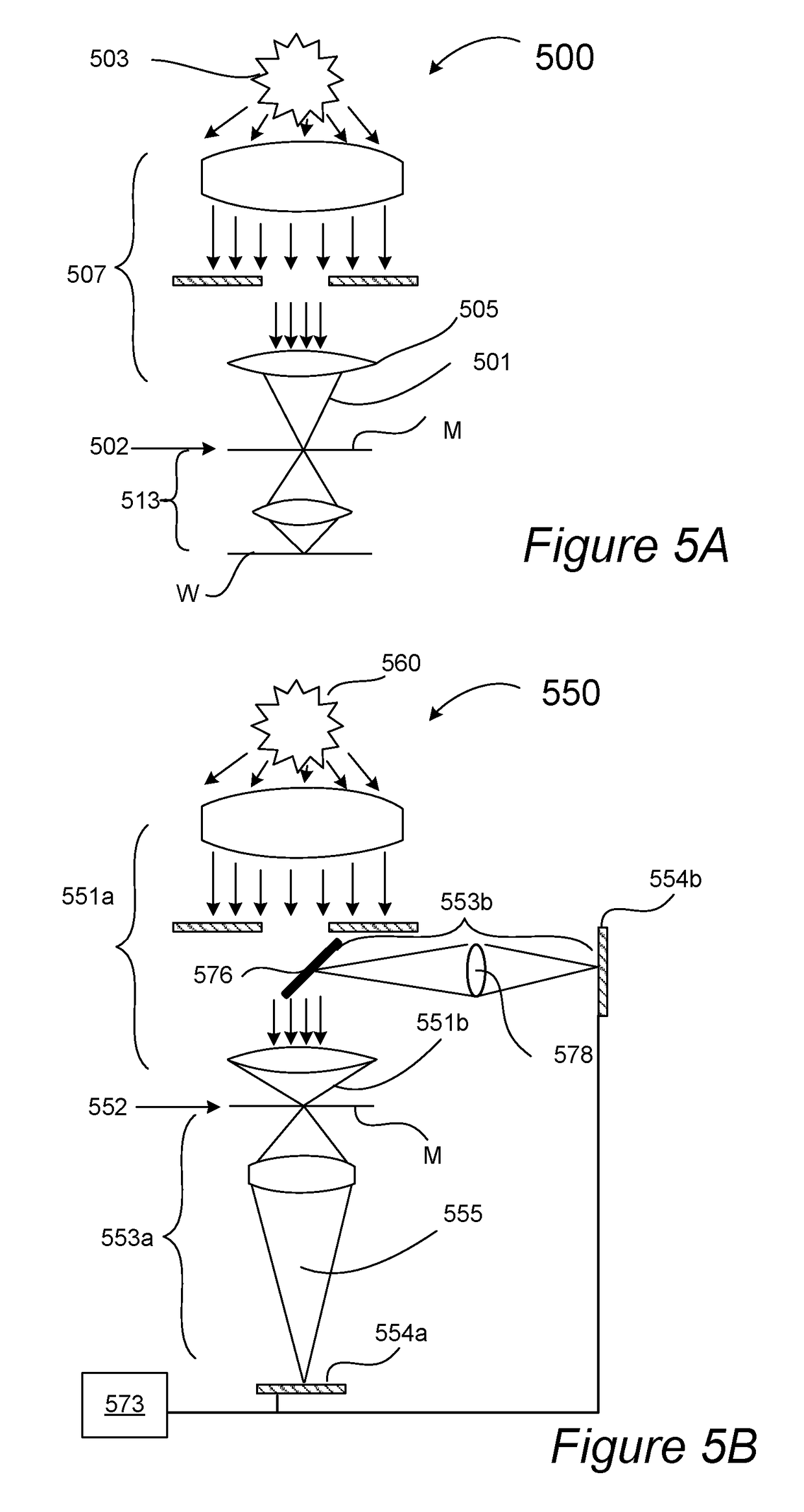
Figure 1 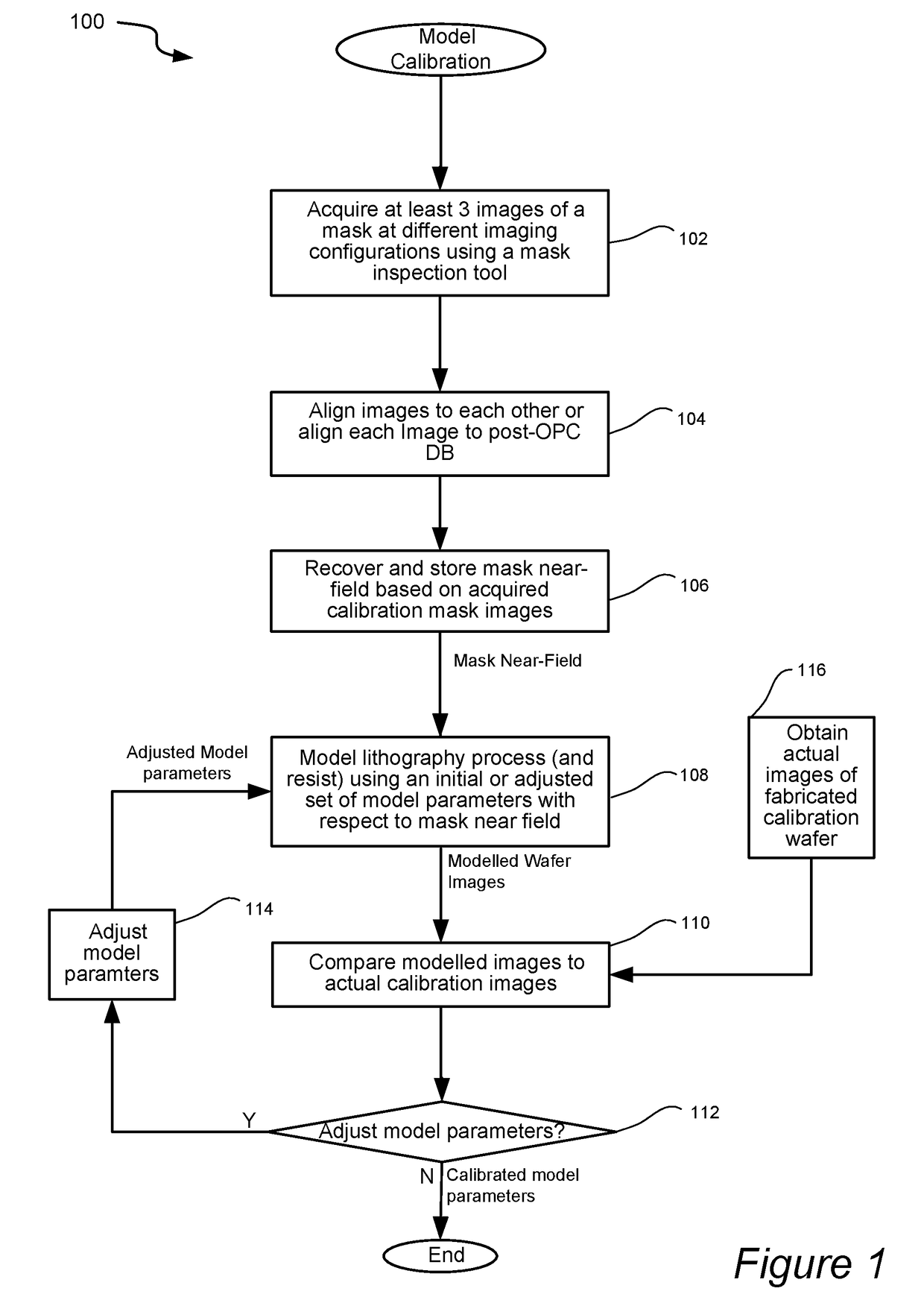
Figure 2 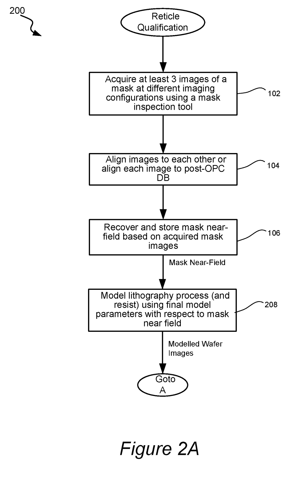
Figure 3
Abstract
Description
CROSS-REFERENCE TO RELATED APPLICATIONS
[0001] This application is a continuation of and claims the benefit under 35 U.S.C. §120 to PCT Application No. PCT / US2016 / 045749, filed Aug. 5, 2016 by Abdurrahman Sezginer et al, which claims the benefit of priority of prior application U.S. application Ser. No. 14 / 822,571, filed 10 Aug. 2015, now U.S. Pat. No. 9,547,892, issued 17 Jan. 2017 by Abdurrahman Sezginer et al. These applications are herein incorporated by reference in their entirety for all purposes.TECHNICAL HELD OF THE INVENTION
[0002] The invention generally relates to the field of reticle inspection. More particularly the present invention relates to pattern qualification.BACKGROUND
[0003] Generally, the industry of semiconductor manufacturing involves highly complex techniques for fabricating integrating circuits using semiconductor materials which are layered and patterned onto a substrate, such as silicon. Due to the large scale of circuit integration and the decreasing size of ...
Examples
Embodiment Construction
[0021]In the following description, numerous specific details are set forth in order to provide a thorough understanding of the present invention. The present invention may be practiced without some or all of these specific details. In other instances, well known process operations or apparatus components have not been described in detail to not unnecessarily obscure the present invention. While the invention will be described in conjunction with the specific embodiments, it will be understood that it is not intended to limit the invention to the embodiments.
[0022]The terms “reticle”, “mask”, and “photomask” are used herein interchangeably and generally each may include a transparent substrate, such as glass, borosilicate glass, quartz, or fused silica having a layer of opaque material formed thereon. The opaque (or substantially opaque) material may include any suitable material that completely or partially blocks photolithographic light (e.g., deep UV). Example materials include c...