
Self-powered ghz solution-processed hybrid perovskite photodetectors
a photodetector and solution processing technology, applied in the field of photodetector systems, can solve the problems of slowing down the low response speed of the solution-processed photodetectors, and little information about the operation speed of the oihp photodetectors, so as to improve the response speed, fast response speed, and charge trap
Patent Information
- Authority / Receiving Office
- US · United States
- Current Assignee / Owner
- Publication Date
- 2018-03-15
Smart Images
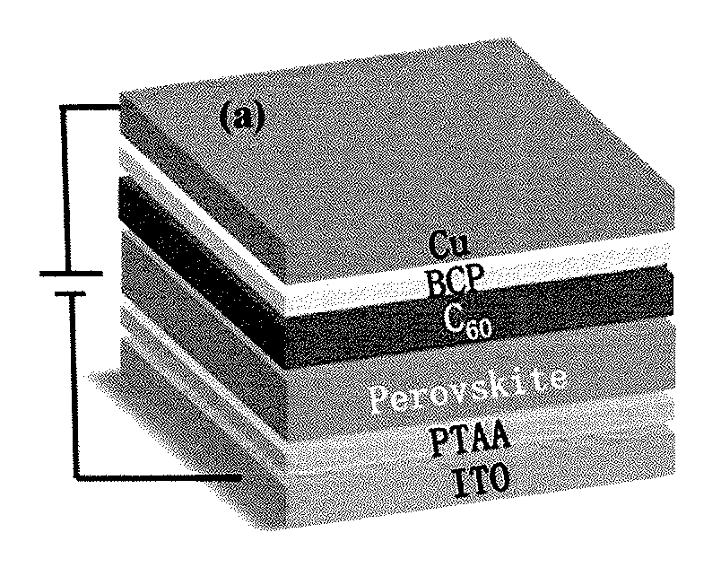
Figure 1 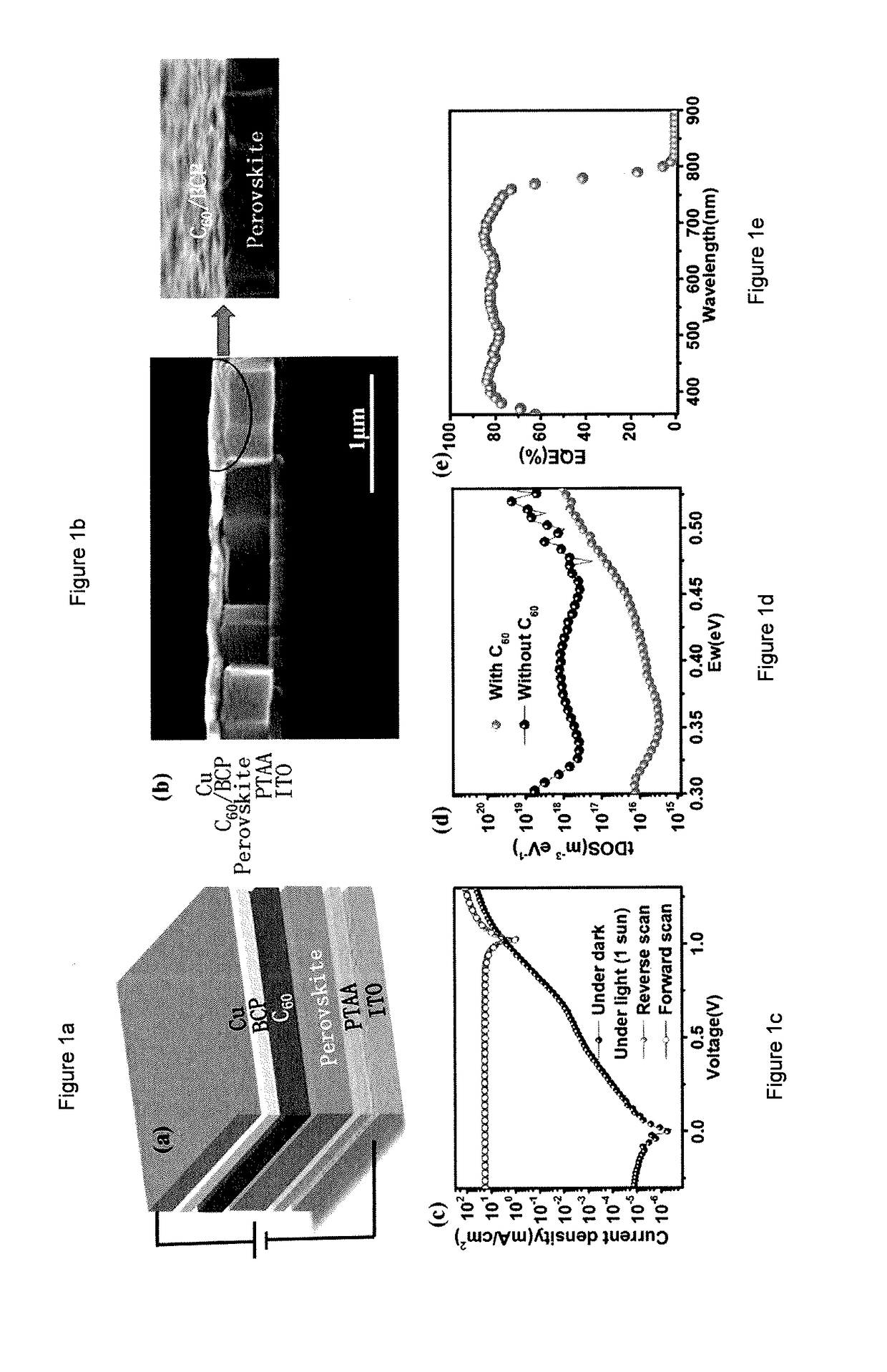
Figure 2 
Figure 3
Abstract
Description
CROSS-REFERENCE TO RELATED APPLICATIONS
[0001] This patent application is a Continuation-in-Part of U.S. Non-provisional Patent Application No. 15 / 009,701, filed Jan. 28, 2016, which claims the benefit of U.S. Provisional Application No. 62 / 108,863, filed Jan. 28, 2015, and is a Continuation-in-Part of U.S. Non-provisional Patent Application No. 14 / 576,878, filed Dec. 19, 2014, (now U.S. Pat. No. 9,391,287), which claims the benefit of U.S. Provisional Patent Application No. 61 / 918,330, filed on Dec. 19, 2013, all of which are incorporated herein by reference. This application also claims the benefit of U.S. Provisional Patent Application No. 62 / 381,412, filed Aug. 30, 2016, which is incorporated herein by reference.FEDERALLY SPONSORED RESEARCH OR DEVELOPMENT
[0002] This invention was made with Government support under contract N000141210556 awarded by The Office of Naval Research, and under contract 2014-DN-077-ARI069-02 awarded by The Department of Homeland Security. The Government ha...
Examples
examples
[0049]Device fabrication. PTAA dissolved in toluene was spun on clean ITO substrates at a speed of 5,000 rounds per minute (rpm). The film was then annealed at 100° C. for 10 min. PbI2 and MAI were dissolved in dimethylformamide (DMF) and 2-propanol with concentrations of 630 mg ml−1 and 65 mg ml−1, respectively. The PbI2 solution was spun on a PTAA layer at 6,000 rpm for 35 s. Then the PbI2 film was transferred onto a hot plate at 90° C. for quick drying. Afterwards, the MAI solution was spun on top of the PbI2 film at 6,000 rpm for 35 s at room temperature, combined with a thermally annealing at 100° C. for 1 h. Finally, the device was completed by thermal evaporating C60 (30 nm), BCP (8 nm) and Cu (80 nm) in sequential order.
[0050]Device characterization.
[0051]AM 1.5G simulated irradiation with an intensity of 100 mW cm−2 was produced by a Xenon-lamp-based solar simulator (Oriel 67005, 150 W) for Current (I)-voltage (V) measurements. The light intensity was calibrated by a silico...