
Physical unclonable functions with copper-silicon oxide programmable metallization cells
a metallization cell and programmable technology, applied in the field of physical unclonable functions with copper-silicon oxide programmable metallization cells, can solve problems such as cracking with sufficient computing power, network intrusion, and denial of service attacks
Patent Information
- Authority / Receiving Office
- US · United States
- Patent Type
- Applications(United States)
- Current Assignee / Owner
- Publication Date
- 2022-05-12
Smart Images
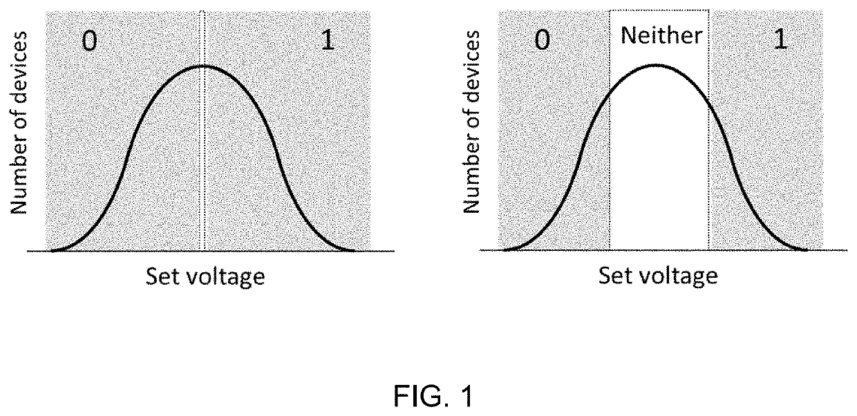
Figure 1 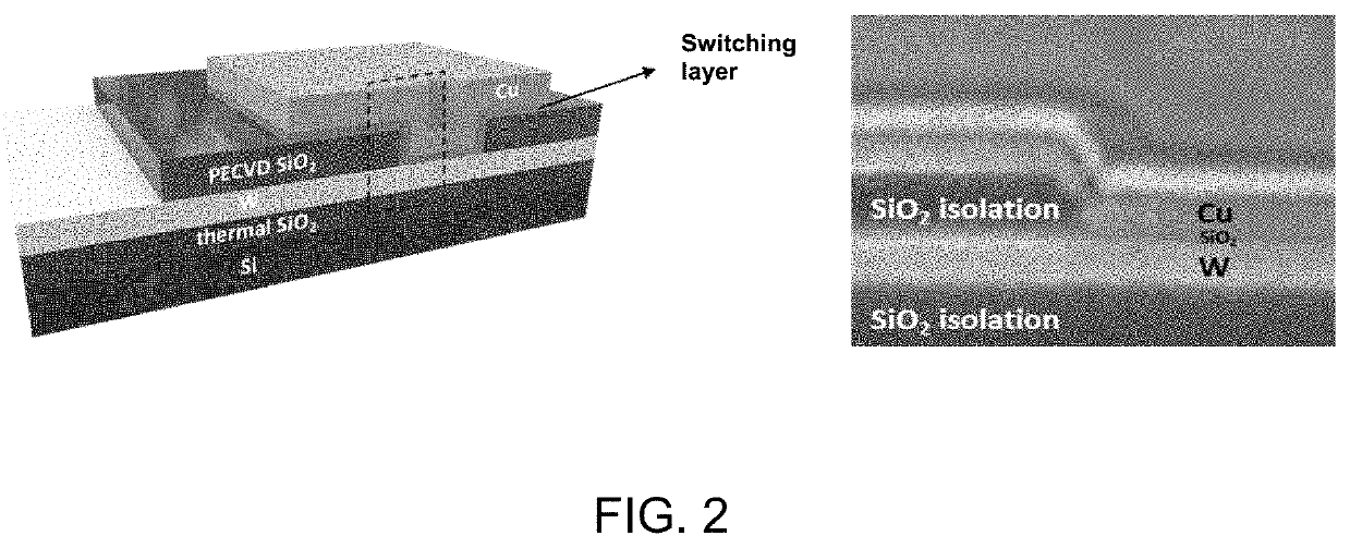
Figure 2 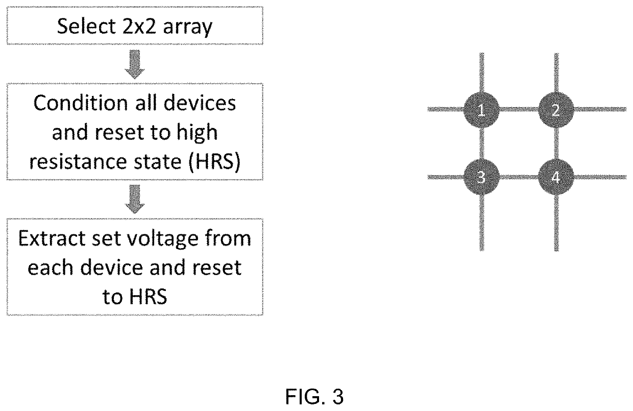
Figure 3
Abstract
Description
CROSS-REFERENCE TO RELATED APPLICATIONS
[0001] This application is a non-provisional of and claims the benefit of U.S. Provisional Patent Application No. 62 / 475,725, filed on Mar. 23, 2017, the contents of which are incorporated herein by reference.BACKGROUND OF THE INVENTION
[0002] Internet security has become increasingly important, in part because of the rapidly growing internet of things (IoT). Many IoT devices are currently communicating on open networks with little or no security, making them vulnerable to network intrusion, including distributed denial of service (DDoS) attacks, for example. Most IoT devices, however, are based on low power system on chip (SOC) designs. Thus, full security on these devices is preferably implemented with as little circuit overhead or additional power consumption as possible to meet operational requirements of the IoT.
[0003] Current secure communications require random number generation to create a secure key. The security of the key is directly rel...
Examples
example
[0056]A device which contains a thin layer of deposited silicon dioxide, silicon oxide, or silica between two electrodes, one of which is copper, can be reversibly switched between high and low resistance states upon application of an appropriate voltage. Subtle differences in operational parameters exist between such devices due to the stochastic nature of the switching process. In particular, the precise voltage at which each device transitions from its high resistance off state to a low resistance on state will vary randomly from device to device. This parameter can be obtained from several devices by electronic means and the results partitioned into ranges representing logic 0 and logic 1, so that an array of devices can generate a random binary word. The word is impossible to predict a priori, as complex and variable atomic scale processes in multiple nanoscale devices are responsible for its generation, but it is simple to read by electrical means. A physical entity that has a...